- The paper introduces a novel method to isolate TLS losses using isotropically etched CPW resonators and participation ratio modeling.
- It employs detailed electromagnetic simulations and Monte Carlo statistical analysis to accurately predict interface and bulk dielectric contributions.
- The findings validate the method's predictive power and suggest design improvements for enhancing superconducting qubit coherence.
Determining Interface Dielectric Losses in Superconducting Coplanar Waveguide Resonators
This paper discusses a precise methodology for quantifying dielectric losses due to two-level systems (TLS) in superconducting coplanar waveguide (CPW) resonators, which is critical for enhancing the performance of superconducting quantum circuits.
Introduction to TLS Losses
Two-level systems are known to significantly impact the performance of superconducting qubits and resonators by introducing energy losses. The paper addresses the challenge of isolating and quantifying the contributions from TLS at different interfaces and bulk materials, which pose a major impediment to optimizing superconducting circuit performance. Previous approaches could either manage to reduce overall TLS loss or only impose bounds on interface losses, failing to distinguish individual contributions effectively.
Methodology for Loss Quantification
The authors employ a combination of statistically characterized CPW resonators and detailed electromagnetic (EM) modeling to discern the TLS loss contributions from multiple interfaces and the bulk silicon substrate. The approach involves using isotropically etched CPW resonators to modulate participation ratios within different interfaces, which allows distinct separation of TLS-induced loss factors correlated with different material interfaces and bulk dielectrics.
The participation ratio model hinges on calculating the electric field energy fraction stored in each dielectric region. This is critical in connecting the loss tangents of these regions (i.e., the extent to which they contribute to energy dissipation) with measurable quantities such as the quality factor (Qi) of the resonators.
Experimental Design and Analysis
The resonators are fabricated on isotropically etched silicon substrates with varied trench depths to accentuate different dielectric region losses. The different resonator designs—each emphasizing a unique dielectric region (MS, SA, MA, or Si)—assist in independently assessing their TLS contributions. Measurements of QTLS are taken at multiple points along the design spectrum to verify the participation-based loss model.
The study employs Monte Carlo simulations to predict the system behavior and determine worst-case uncertainties associated with the extracted loss factors.
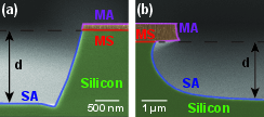
Figure 1: Cross-sectional SEM images distinguishing metal-to-substrate, substrate-to-air/vacuum, metal-to-air/vacuum, and bulk silicon regions.
Results and Discussion
The results from EM simulation and statistical characterization are verified against the measured TLS-limited quality factors (QTLS) of additional, distinct geometries. This demonstrates the model's predictive power and its utility as a diagnostic tool for assessing the source of TLS losses.
The study concludes that isotropic trenching in CPW designs lowers the uncertainty in determining dielectric-specific losses compared to earlier methodologies using anisotropic trenching. Figures show that with sufficient device quantities (roughly equivalent to two dilution refrigerator cool-downs), meaningful isolation and quantification of individual dielectric losses can be achieved.
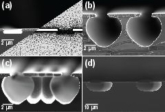
Figure 2: SEM imaging and COMSOL mesh examples for CPW resonator geometries designed to emphasize specific dielectric losses.
Conclusion
By achieving a unique determination of interface loss tangents in superconducting microwave resonators, this research furnishes an instrumental model for predicting losses, setting the stage for advances in qubit and resonator design. Knowledge of these specific loss contributions could facilitate precise fabrication process enhancements and the evaluation of different materials or procedures aimed at minimizing TLS impacts. This represents a step forward in improving the coherence time of superconducting qubits and the quality factor of resonators, essential for scaling quantum computing architectures.
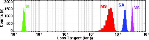
Figure 3: Predicted vs. measured QTLS for various resonator designs, validating the participation ratio model's accuracy.