- The paper presents a novel on-surface synthesis integrating BN-doped rubicene into graphene nanoribbons via a hierarchical Ullmann coupling protocol.
- High-resolution STM, AFM, and DFT analysis verify the structure, defect control, and substantial band gap opening to ~1.7 eV.
- The findings offer a versatile platform for tunable optoelectronic applications and precise defect engineering in nanographenic materials.
Atomically Precise Synthesis of BN-Doped Rubicene in Graphene Nanoribbons
Introduction
The incorporation of heteroatoms and non-benzenoid motifs into graphene nanoribbons (GNRs) offers a pathway for precise atomic engineering of electronic properties, including modulation of the band gap and magnetic or optoelectronic functionalities. This work presents a bottom-up, on-surface synthesis of GNRs featuring embedded, fused BN-doped rubicene units on Au(111), providing a versatile platform for the rational design of semiconducting GNR architectures with tailored properties. The study utilizes a combination of scanning tunneling microscopy (STM), atomic force microscopy (AFM) with CO-functionalized tips, and density functional theory (DFT) calculations for full structural and electronic characterization.
Synthetic Route and Structural Elucidation
The synthesis leverages a hierarchical Ullmann coupling protocol. Halogenated 7,16-dibromo-5,14-dihydro-5a,14a-diaza-5,14-diboradibenzo[a,m]rubicene (B2N2-DBR) is deposited onto Au(111) under UHV, followed by thermal activation. Initial annealing at T1≈160∘C induces polymerization into poly-B2N2DBR chains; further annealing at T2≈250∘C triggers cyclodehydrogenation, generating planar BN-GNRs with rubicene moieties periodically embedded.
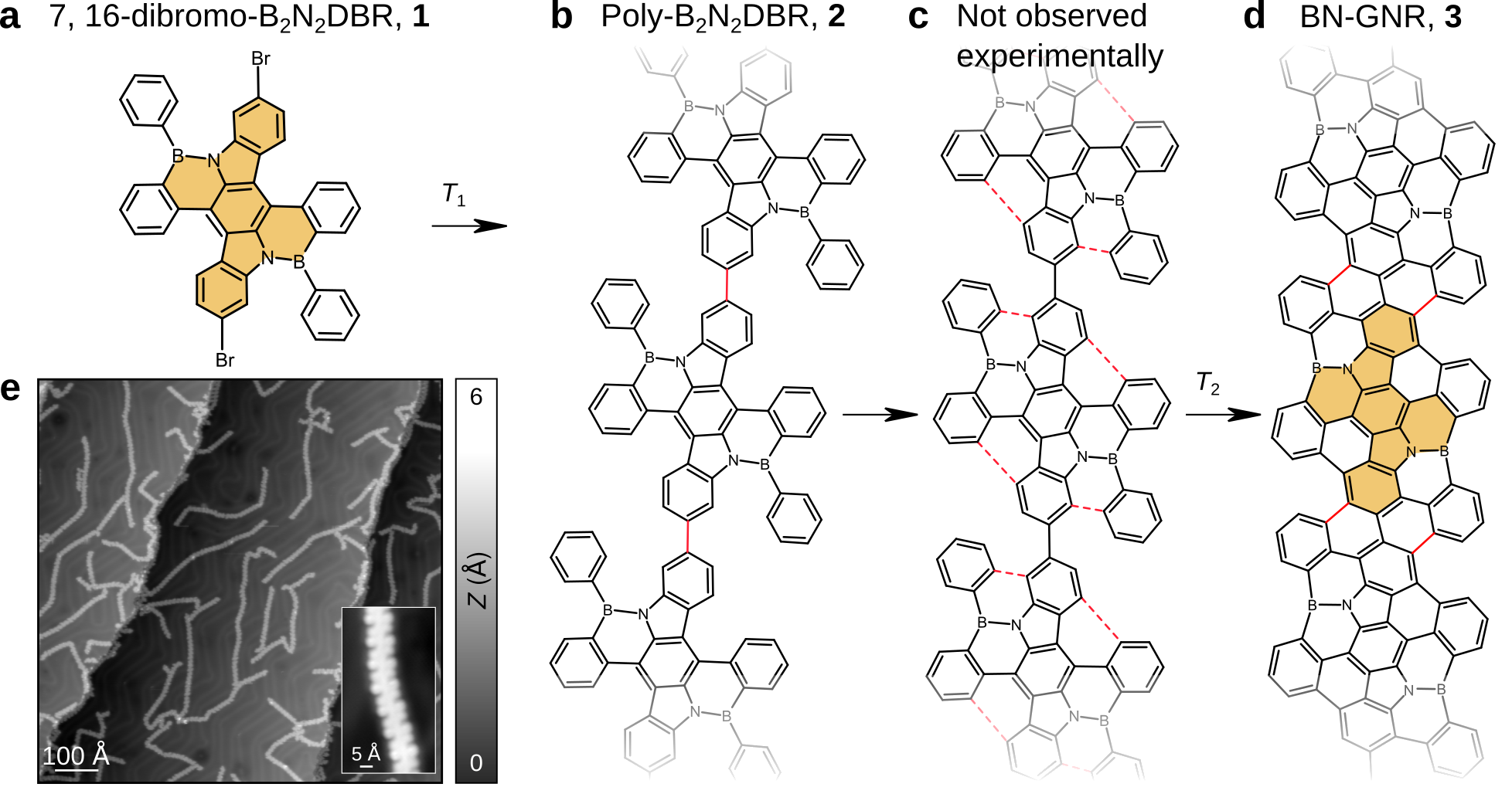
Figure 1: Synthetic route for BN-GNRs, including precursor design, Ullmann coupling, and cyclodehydrogenation to generate periodic BN-rubicene units within GNRs.
High-resolution STM and AFM imaging confirm the integrity and periodicity of the BN-doped structures and validate the efficient planarization of peripheral phenyl groups upon cyclodehydrogenation. DFT-relaxed structures, supported by simulated AFM contrast, align with the observed ribbon contour and BN-doping sites.
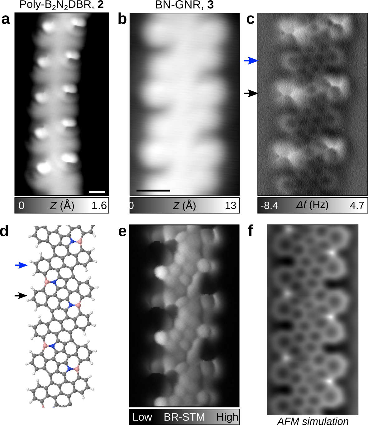
Figure 2: AFM and STM characterization of BN-GNRs, matching DFT-optimized structures with experimentally observed features and confirming BN site localization.
Defect Analysis and Reaction Pathways
Defect engineering is critical for device reliability and is extensively analyzed here. The defect density in BN-GNRs correlates with the thermal annealing protocol; slow ramp rates yield up to 90% defect-free domains, while rapid ramps increase defect incidence to 30–35%. AFM discriminates between pristine and defect-laden segments, revealing both BN-hexagon and B-pentagon motifs, with the former thermodynamically stabilized by ∼1.4 eV relative energy.
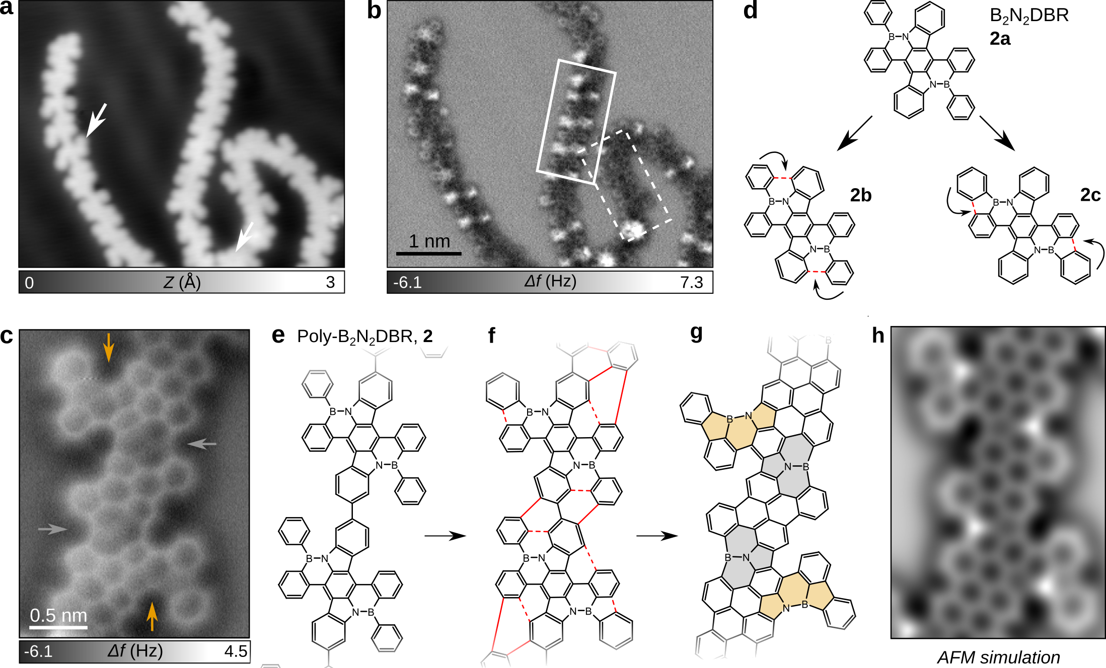
Figure 3: AFM and STM visualize structural defects, traced to alternative cyclodehydrogenation pathways and varying BN ring topologies; simulations confirm experimental features.
DFT analysis suggests that high-temperature, fast-anneal pathways are potentially mediated by Au adatoms, increasing regioselectivity toward less stable BN-site configurations. This nuance is instrumental for future synthetic strategies targeting low-defect topologies.
Electronic Structure: Band Gap Engineering
Differential conductance (STS) and DFT band structure calculations consistently demonstrate a substantial electronic band gap opening upon periodic inclusion of BN-rubicene units. The BN-GNR band gap in vacuum is calculated to be 1.55 eV and observed by STS to be ∼1.7 eV on Au(111), compared to the undoped counterpart's significantly lower gap. Doping also induces dispersive valence and conduction bands crucial for optoelectronic device integration.
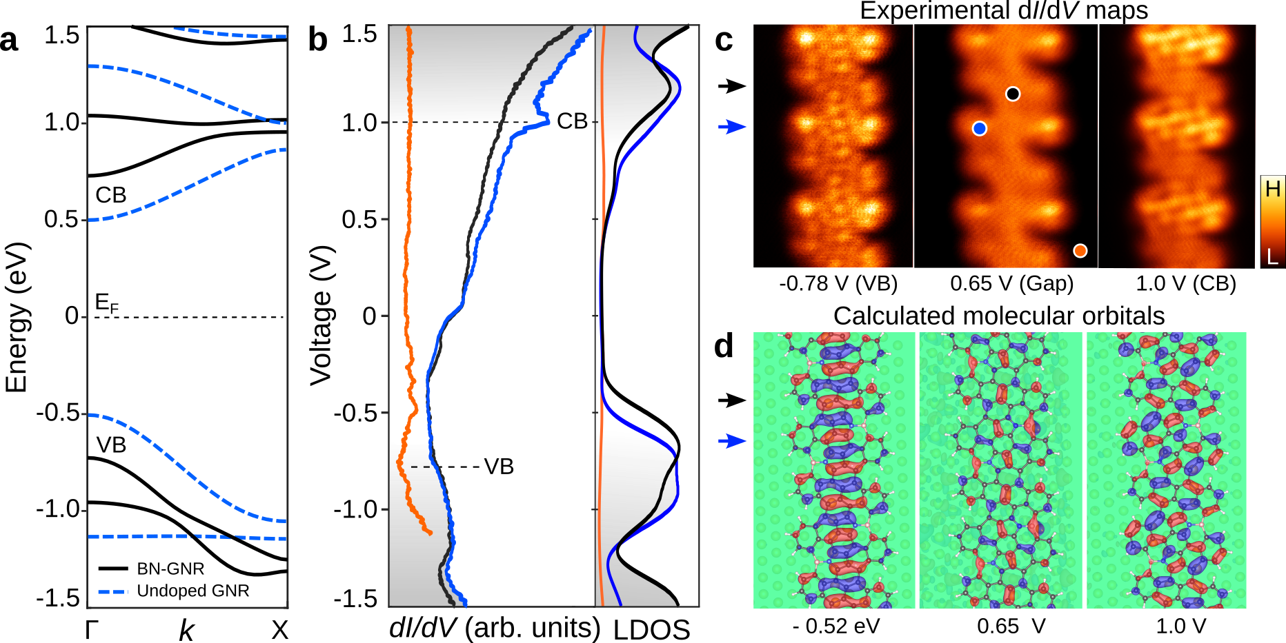
Figure 4: DFT band structure (gas phase) and spatially resolved STS maps, showing substantial band gap opening and state localization over BN-rubicene units.
The local density of states is highly modulated, with VB and CB maxima localized over fused BN-doped rubicene units, a signature distinct from pristine GNRs. Experimental dI/dV maps reproduce DFT orbital distributions, validating the predicted frontier orbital topology and semiconducting character.
Implications and Future Prospects
The atomically controlled integration of BN-doped rubicene within GNRs enables tunable band gap engineering through heteroatomic and non-benzenoid design. This work demonstrates that precise BN distribution, beyond simple substitution, can achieve significant functional modulation, providing a platform for optoelectronic applications, including solution-processable semiconductors and photovoltaic materials. The high-fidelity match between theory and experiment establishes protocols reusable in the directed synthesis of other atomically doped or defect-modulated nanographenic systems.
The practical control over defect densities, via process modulation, further enhances device fabrication reliability, and the adaptability of the process to other lattice-engineered systems is clear. Electrically decoupled studies, as proposed, will clarify the optical response and charge carrier behavior for device contexts.
Conclusion
Atomically precise BN-GNRs with periodic BN-doped rubicene units have been synthesized and characterized, showing substantial band gap opening and robust semiconducting behavior. A synergistic approach combining STM/AFM, STS, and DFT provides a comprehensive characterization of both structure and electronic properties. The BN-GNR architecture is a promising candidate for next-generation optoelectronic applications, with synthetic versatility extending to other heteroatom and non-benzenoid nanographenic materials (2306.07586).

