- The paper achieves a lower propagation loss of 1.03 dB/cm compared to typical ScAlN losses exceeding 2.4 dB/cm.
- It employs molecular beam epitaxy and optimized waveguide design via simulation to enhance light confinement and device performance.
- Experimental results demonstrate intrinsic quality factors over 3×10^5, revealing the platform's potential for scalable photonic integrated circuits.
Hybrid Scandium Aluminum Nitride/Silicon Nitride Integrated Photonic Circuits
Introduction
The integration of high-performance photonic devices requires materials that balance low optical loss with advanced electromagnetic functionalities. Scandium-doped aluminum nitride (ScAlN) emerges as a promising candidate for quantum photonic integrated circuits (PICs) due to its strong second-order nonlinearity, ferroelectricity, piezoelectricity, and CMOS compatibility. Despite its potential, ScAlN typically suffers from optical losses exceeding 2.4 dB/cm. This paper presents a novel monolithically integrated \ce{Si3N4}âScAlN waveguide platform that addresses this challenge by achieving a propagation loss of 1.03 dB/cm, comparable to commercial silicon-on-insulator (SOI) waveguides.
Material Growth and Characterization
This study leveraged molecular beam epitaxy (MBE) to grow single-crystalline ScAlN on a sapphire substrate, using AlN as a buffer layer to minimize dislocations and optical losses. The surface roughness is characterized at 1.2 nm, ensuring minimal scattering. Cross-sectional STEM and EDS analysis (Figure 1) confirms the seamless integration of the ScAlN layer, facilitating optical comparison with conventional single-mode waveguides.
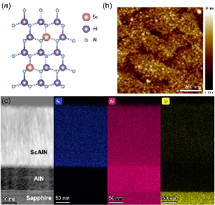
Figure 1: Materials characterization of ScAlN.
Device Design and Numerical Simulation
The \ce{Si3N4}-ScAlN hybrid waveguide design aims to optimize light confinement and minimize bending loss. Geometry simulations reveal significant confinement in ScAlN despite reduced layer thickness compared to \ce{Si3N4}, notably improving propagation dynamics. Simulations of the fundamental TE and TM mode distributions (Figure 2) underpin the strategic design, balancing optical performance across different polarizations.
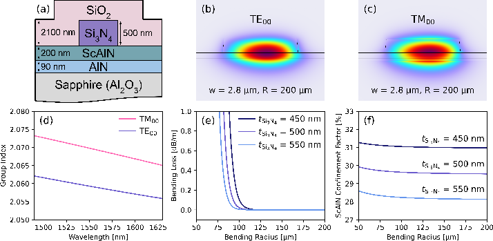
Figure 2: Waveguide design and simulated optical characteristics.
Experimental Results
Fabrication: Utilizing an innovative amorphous silicon (a-Si) hardmask etching process, the photonic chips were fabricated with smooth \ce{Si3N4} sidewalls. SEM images demonstrate the device quality and sidewall sharpness necessary for minimizing optical propagation loss (Figure 3).
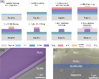
Figure 3: Fabrication of the \ce{Si3N4âScAlN photonic chips.
Optical Loss Characterization: The propagation loss measurements yielded an intrinsic quality factor Qi exceeding 3×10⁵, cutting edge for ScAlN-based platforms. Detailed characterization through transmission spectra (Figure 4) showcases the optical resilience of the resonator designs, including Euler racetrack constructions that optimize cavity geometry for lower loss and higher quality factors.
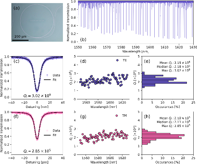
Figure 4: Optical loss characterization of the circular microring resonator.
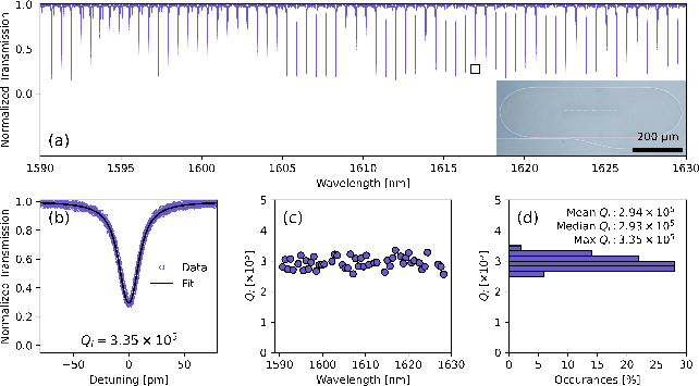
Figure 5: Optical loss characterization of the Euler racetrack microring resonator.
Conclusion
The hybrid \ce{Si3N4}-ScAlN platform epitomizes a significant advancement in low-loss photonics, achieving quality factors analogous to commercial SOI technologies while offering ferroelectric and piezoelectric functionalities. With prospective enhancements via hydrogen bond reduction in \ce{Si3N4}, the architecture paves the groundwork for scalable photonic systems in data communication and AI-driven applications, aligned with CMOS fabrication processes.
This monolithic approach posits ScAlN as a premier candidate within photonic systems, presenting strong implications for future enhancements in optical communication, modulation, sensing, and quantum computing. The study underscores not only the practical merit of combining ScAlN with \ce{Si3N4} but also foreshadows broader implications for next-generation PICs.