- The paper demonstrates efficient coupling of SnV centers to one-dimensional photonic crystal cavities via advanced thin-film diamond nanofabrication, achieving Purcell factors exceeding 26.
- The methodology combines He²⁺ implantation, epitaxial CVD overgrowth, and precise nanobeam patterning to align cavity resonances with the SnV zero-phonon line near 619 nm.
- The study validates a scalable quantum network platform by extracting detailed branching ratios and identifying key fabrication parameters such as angular misalignment.
Quantum Nanophotonic Interface for Tin-Vacancy Centers in Thin-Film Diamond
Introduction and Motivation
The manuscript presents an experimental and analytical study of SnV− color centers in thin-film diamond, interfaced with one-dimensional photonic crystal cavities engineered for efficient nanophotonic coupling. The overarching motivation is to exploit the superior optical and spin properties of SnV− centers for scalable quantum network nodes: SnV− offers robust spin coherence at liquid helium temperatures due to its large ground-state splitting (∼850 GHz), outperforming SiV− and NV− in electric field noise insensitivity and ZPL emission fraction. The work directly addresses the challenge of integrating SnV− centers into high-Q nanophotonic structures compatible with on-chip quantum network architectures, using thin-film diamond rather than bulk carving techniques.
Thin-Film Diamond Preparation and Nanofabrication
Thin-film diamond membranes were produced using combined He2+ ion implantation, epitaxial CVD overgrowth, and electrochemical etching. Sn2+ ions were implanted into the fresh epitaxial layer to generate SnV− centers at a depth of ∼90 nm, followed by high-temperature annealing and chemical treatments for defect activation and surface cleanup. Nanobeam photonic crystal cavities (beam width 300 nm, hole diameter 115 nm) were patterned and etched with high fidelity, with both parallel and angled orientations with respect to the ⟨100⟩ diamond axis. Lattice spacings were systematically swept (180-210 nm, ∼2.5 nm steps) for resonance matching near the 619 nm ZPL.
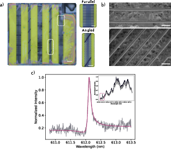
Figure 1: SEM and optical characterization of parallel and angled cavity nanobeams, showing high-fidelity patterning, measured quality factor, and resonance spectrum.
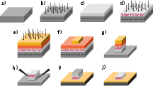
Figure 2: Schematic of thin-film diamond preparation including polishing, He2+ implantation, CVD overgrowth, Sn2+ implantation, membrane exfoliation, and etch steps.
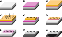
Figure 3: Process flow for nanobeam cavity fabrication by e-beam lithography, hardmask transfer, etching, and membrane suspension.
Device Characterization and Optical Interface
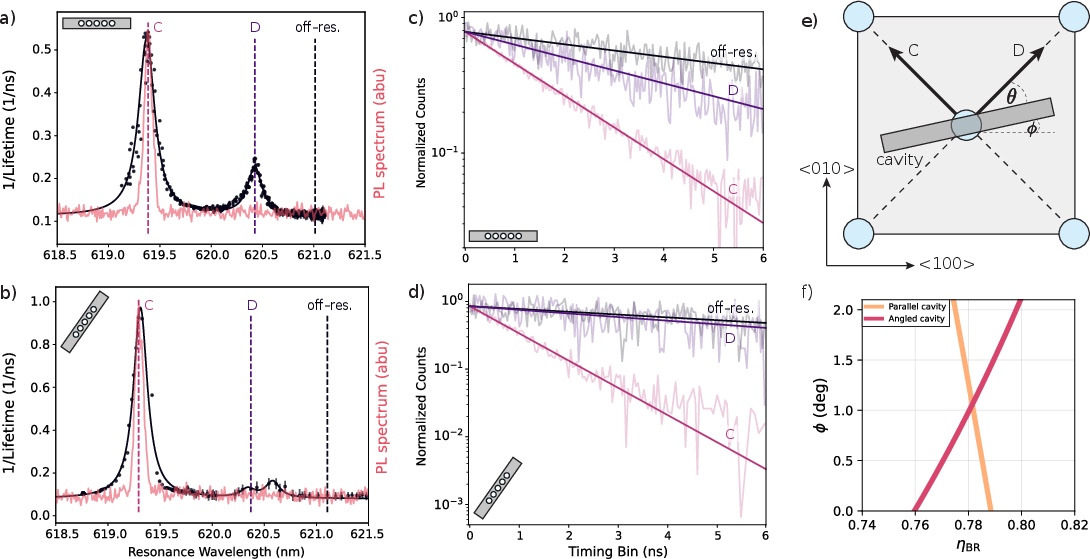
At 4 K, cavity resonances were probed via cross-polarized reflectivity, with measured quality factors up to ∼6000 for the best devices (6032 for parallel, 3942 for angled). Photoluminescence (PL) confocal microscopy and gas-tuning were employed to align cavity modes with the SnV− ZPL transitions (C and D), achieving up to 10-fold PL intensity enhancement on resonance in parallel cavities and 2.5-fold in angled devices.
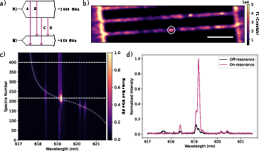
Figure 4: SnV− energy level structure, PL confocal scan of an emitter cluster in a cavity, demonstration of cavity-induced PL enhancement.
Spectroscopy identified clusters of 2-3 emitters per cavity mode due to high implantation dose. The optical setup, employing a 4f confocal microscope, tunable lasers, and time-correlated photon counters, enabled precise spectral and time-domain measurements.
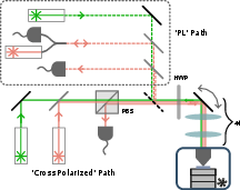
Figure 5: Schematic of optical measurement setup detailing dual-path excitation/collection, cryogenic sample mounting, and photon detection.
Purcell Enhancement and Spontaneous Emission Analysis
Time-resolved PL measurements quantified emitter lifetimes for both C and D ZPL transitions. Lifetime reductions were significant:
The Purcell factor F was rigorously calculated using an explicit model for collective spontaneous emission, incorporating orthogonal dipole moments, cavity alignment (θ), spatial positioning, and Debye-Waller factor (ηDW=0.57). The branching ratio ηBR of emission rates for C/D transitions was simultaneously extracted. Values obtained:
- Parallel cavity: FC=9.243±0.001, FD=8.910±0.0001
- Angled cavity: FC=26.21±0.01, FD=5.12±0.05
- Consistent branching ratio: ηBR=0.7815
- Fabrication angular misalignment: ϕ=1.1±0.1∘
The analysis underscores the critical dependence of cavity enhancement on both dipole-cavity orientation and device angular alignment, with simulations predicting maximal improvement (∼40%) for 45∘ cavity orientation.
Implications for Quantum Networks and Spin-Photon Interface
The study demonstrates that precise alignment and nanofabrication in thin-film diamond enables substantial Purcell enhancement and efficient photon extraction from SnV− centers. This has direct implications for quantum network nodes, where high-fidelity single-shot optical spin readout is predicated on ZPL emission and cavity coupling. The extraction of the intrinsic C/D branching ratio from time-domain measurements provides a more fundamental characterization than indirect PL methods.
Furthermore, the platform is compatible with microwave spin control and photonic integration strategies (grating couplers, tapers), and could be improved via lower implantation densities and aligned implantation. These optimizations are projected to further enhance the Purcell factor and emitter-cavity coupling, supporting scalable multiplexing and integration of quantum memories and processing nodes.
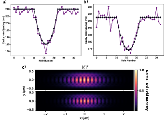
Figure 7: Analysis of nanofabrication fidelity and cavity simulation showing field confinement and angular deviations relative to designed geometry.
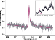
Figure 8: Reflectivity spectrum and quality factor measurement for angled cavity, demonstrating Fano resonance fitting.
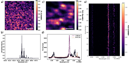
Figure 9: PL and PLE mapping of thin-film emitters pre-fabrication, quantifying SnV− formation and addressing linewidths.
Conclusion
The manuscript elucidates the fabrication, characterization, and fundamental optical physics governing tin-vacancy center coupling in nanophotonic diamond cavities. Key results include quality factors up to ∼6000, Purcell factors exceeding 26 for optimal transitions, and a reliable method for extracting both branching ratios and device angular misalignments. The reported approach enables high-fidelity quantum interfaces with solid-state spin-photon platforms, positioning thin-film diamond as a viable substrate for scalable quantum networking.
Future research should focus on deterministic emitter placement, further geometric control of cavity fields, passivation of surface-related noise, and integration with photonic circuits for spin multiplexing. The techniques and analyses delivered here form a robust framework for real-world implementation of quantum network nodes using group-IV color centers in diamond.