Photonic Waveguide Circuit Integrated with Carbon Nanotube Single-Photon Source Operating at Room Temperature
Abstract: Photonic integrated circuits require robust room-temperature single-photon sources to enable scalable quantum technologies. Single-walled carbon nanotubes (CNTs), with their unique excitonic properties and chemical tunability, are attractive candidates, but their integration into photonic circuits remains challenging. In this work, we demonstrate the integration of functionalized CNTs as room-temperature single-photon emitters into photonic cavities and waveguide circuits. (6,5) CNTs with aryl sp$3$ defects are either stochastically deposited via drop-casting or deterministically positioned on photonic cavities using an anthracene-assisted transfer method guided by real-time photoluminescence monitoring. Photoluminescence spectra reveal cavity-enhanced emission, while second-order autocorrelation measurements confirm single-photon propagation through the photonic integrated circuit, highlighting the potential of CNTs for scalable, room-temperature quantum photonic applications.
Paper Prompts
Sign up for free to create and run prompts on this paper using GPT-5.
Top Community Prompts
Explain it Like I'm 14
Plain-English Summary of the Paper
What is this paper about?
This paper shows how to build a tiny “light circuit” on a chip that can carry single particles of light—called photons—at room temperature. The special light source is made from carbon nanotubes (CNTs), which are like super-thin straws made of carbon. The team managed to place these nanotubes onto tiny light-guiding structures so the chip can generate, control, and route single photons, which is important for future quantum technologies.
What are the main questions the researchers asked?
- Can we get carbon nanotubes to act as reliable single-photon sources on a chip at normal room temperature (no big freezers needed)?
- Can we connect these nanotubes to tiny “roads for light” (waveguides) and “light echo chambers” (cavities) so the single photons they emit can be guided and used in a photonic circuit?
- Can we place the nanotubes on the chip in a simple way (quick but random) and in a precise way (careful but accurate), and will both methods work?
How did they do it? (Explained with simple ideas)
First, a few key ideas:
- Photonic integrated circuits (PICs): Think of a city map, but instead of roads for cars, there are waveguides—tiny glassy paths that guide light around a chip.
- Waveguides: Tiny “pipes” that carry light from one place to another.
- Cavities: Tiny “echo chambers” for light that amplify or sharpen certain colors.
- Single photons: Light sent one particle at a time—useful for quantum communication and computing.
- Carbon nanotubes (CNTs): Ultra-thin tubes of carbon that can glow when excited by a laser.
- “Defects” in CNTs: Carefully added tiny “traps” that help a CNT emit one photon at a time, clearly and reliably.
What they built and tested:
- They chose a material called lithium niobate (LiNbO3) to make the chip. It’s good because it doesn’t glow on its own in the infrared (so it won’t drown out the signal) and it can be electrically tuned later.
- They designed and fabricated waveguides, grating couplers (to get light in and out of the chip), and special cavities that match the color of light the CNTs emit (around 1250–1300 nm, which is useful for telecom fiber networks).
- They prepared (6,5) carbon nanotubes with special “sp3 defects” so they naturally emit single photons at room temperature.
How they put the CNTs on the chip:
- Quick method (drop-casting): They dropped a tiny liquid containing CNTs onto the chip. It’s fast but the nanotubes land randomly.
- Precise method (anthracene-assisted “stamping”): Imagine using a sticky but clean stamp (made with a crystal called anthracene on a soft pad) to pick up a nanotube and press it exactly onto the cavity on the chip. They monitored the glow (photoluminescence) in real time to line things up, then gently warmed the chip so the anthracene disappears, leaving a cleanly placed nanotube.
How they checked it worked:
- They shined a laser on the CNT to make it glow (photoluminescence).
- The light went into the cavity and then into the waveguides.
- At the ends of the waveguides, they used fibers connected to very sensitive single-photon detectors.
- They performed a “photon autocorrelation” test. In simple terms, this test checks whether the light is coming one photon at a time. A key number, g2(0), closer to 0 means “more single-photon-like,” while above 0.5 means “not single photons.”
What did they find, and why does it matter?
Main results (kept simple and focused):
- The carbon nanotubes sent their light into the chip’s cavity and waveguides at room temperature.
- The cavity made the light spectrum sharper (more focused in color), which helps for building precise optical circuits.
- The single-photon test showed very strong single-photon behavior: g2(0) ≈ 0.08 and 0.10 in their best devices (well below 0.5), meaning the light comes out one photon at a time.
- Both methods of placing CNTs worked:
- Drop-casting (fast but random) still produced single photons in the circuit.
- Stamping (careful and accurate) also worked and is better for building larger, organized circuits.
Why this is important:
- Doing this at room temperature is a big deal. Many quantum light sources only work when cooled to very low temperatures, which is costly and bulky.
- The CNTs can emit in the telecom range (the “colors” used in fiber-optic internet cables), which makes it easier to connect quantum chips to existing communication networks.
- It shows a promising path to making scalable, chip-based quantum devices that can be mass-produced.
What are the limits now, and what’s next?
- Some losses still exist when coupling light in and out of the chip (through the “grating couplers”), and the waveguides themselves can be improved to reduce loss.
- The current cavity design didn’t speed up the CNT emission much (a “Purcell boost”), mainly because the light mode is relatively large and the overlap with the nanotube could be better. Smaller, better-matched cavities could greatly increase brightness—possibly by around 150× with improved designs.
- The CNTs can show “blinking” or degrade under strong pulsed lasers; improving stability and placement methods will help.
So, what’s the big picture?
This work is a step toward practical quantum photonic chips that work at normal room temperatures. By proving that carbon nanotubes can be cleanly integrated and deliver single photons into tiny on-chip light circuits, the researchers opened the door to future devices for:
- Quantum communication (more secure messaging)
- Quantum sensors (very sensitive measurements)
- Quantum information processing (steps toward quantum computing)
In short, they’ve shown a clear, workable recipe for building single-photon circuits on a chip, using parts that fit well with real-world telecom technology.
Knowledge Gaps
Knowledge gaps, limitations, and open questions
The paper demonstrates room-temperature coupling of CNT single-photon emission into lithium niobate (LN) photonic circuits, but leaves several concrete gaps and unresolved questions that future work could address:
- Absolute efficiency and rate: No calibrated measurement of end-to-end efficiency (emitted photons per second into the guided mode and into the output fiber) is provided; the “~30% coupled” estimate is unvalidated. Establish a standardized metrology of source brightness, chip-to-fiber coupling, and detector-chain efficiency.
- Background and noise: The contribution of LN background PL, scattered pump light, grating-coupler leakage, and detector dark counts to g2(0) is not quantified. Implement on-chip spectral filtering and systematic background subtraction to determine SNR and its impact on single-photon purity.
- Stability and degradation mechanisms: CNT emitters show blinking and rapid degradation under pulsed excitation (minutes to hours), with causes unresolved. Identify dominant mechanisms (e.g., local heating, photo-oxidation, surfactant effects, polymer residues) and evaluate encapsulation (hBN, ALD oxides), environmental control (humidity/oxygen), and excitation schemes to improve operational lifetimes.
- Purcell enhancement: No observable lifetime shortening is reported; the Purcell factor is estimated to be low (~0.34) due to large mode volume and limited overlap. Realize air-mode, small–mode-volume cavities; quantify actual lifetime changes, emission rate enhancement, and spatial/polarization overlap ξ.
- Emitter–cavity alignment and orientation: The tube orientation relative to cavity polarization is not measured or controlled post-transfer. Develop methods to orient CNTs (e.g., alignment fields, trench guidance) and quantify coupling dependence on angular misalignment.
- Residues and cavity Q degradation: Cavity Q degrades after CNT transfer, attributed to polymer wrapping or transfer residues, but contamination is not directly characterized. Implement and verify residue-free transfer (e.g., improved anthracene sublimation, solvent/UV-ozone cleaning), and measure pre/post-transfer Q and resonance shifts to model optical loading by CNTs.
- Deterministic placement yield and process control: Anthracene-assisted stamping has ~25% success, with PDMS retraction as a bottleneck and non-planarity issues. Engineer stamp mechanics (planar microfabricated stamps, controlled adhesion surfaces), automate alignment under in-situ PL, and report placement accuracy (lateral/rotational) and yield statistics.
- Post-deposition waveguide losses: The impact of CNT placement and residues on waveguide propagation loss is not measured. Quantify loss changes after CNT integration and identify scattering/absorption contributions to inform process improvements.
- Grating coupler efficiency vs emitter access: Current GC loss (~–9 dB) limits throughput; proposed improvements (claddings, bottom reflectors, chirped/subwavelength GCs) conflict with the need for exposed waveguides for CNT coupling. Design locally windowed claddings or heterogeneous stacks to boost GC efficiency while preserving emitter access; validate experimentally.
- Electro-optic tuning: LN’s EO capability is not leveraged to tune cavity resonances to track CNT emission drift. Integrate electrodes, measure tuning ranges/speeds, and implement feedback to maximize spectral overlap and coupling.
- Telecom C-band operation: Demonstration is at ~1250–1300 nm; extension to ~1550 nm (C-band) using larger-diameter chiralities and matching cavity/coupler designs remains untested. Evaluate performance, purity, and stability across O-, S-, and C-bands.
- Electrical excitation: The work uses optical pumping; electrically driven CNT single-photon sources on LN are not demonstrated. Integrate electrodes compatible with LN (and CNT contact schemes), and measure electroluminescence purity, brightness, and stability at room temperature.
- Coherence and indistinguishability: No measurements of spectral diffusion, homogeneous linewidth, T2, or two-photon interference (HOM) are reported. Characterize linewidths in-cavity, assess indistinguishability, and explore cavity filtering/tuning to approach coherent emission.
- Pumping strategies: Pulsed excitation accelerates acquisition but damages emitters; CW excitation is slow. Test resonant pumping, cavity-enhanced absorption, and mixed-dimensional exciton transfer (e.g., via 2D semiconductors) to reduce pump intensity while maintaining count rates.
- Multi-emitter scaling and statistics: Results highlight “best” devices; ensemble statistics (yield of g2(0)<0.5, brightness distributions, spectral alignment yields) are missing. Build arrays, report device-to-device variability, and identify process parameters governing reproducibility.
- On-chip HBT and detection: The HBT relies on external SNSPDs and fiber filters; fully integrated detectors and filters on LN (or hybrid integration) are not explored. Demonstrate on-chip HBT to reduce losses, and quantify crosstalk and background in integrated architectures.
- Polarization control on-chip: The polarization state of guided single photons is not measured or controlled. Characterize polarization after the cavity and implement polarization-maintaining waveguides/converters if needed for downstream quantum circuits.
- Thermal effects: Local heating under excitation and its impact on spectral drift, degradation, and g2(0) are unquantified. Measure temperature rise (e.g., Raman thermometry), implement thermal management (heat sinking), and determine safe operating regimes.
- Functionalization chemistry and defect density optimization: The trade-offs between defect density, purity, brightness, and PIC compatibility (aqueous vs organic dispersions, surfactants) are not mapped. Systematically vary defect densities and chemistries to optimize integrated performance.
- Cavity design trade-offs: Mode splitting and higher-order modes are suppressed via small grating-period changes, but a comprehensive design space exploration is absent. Optimize cavity geometry for single-mode operation, high Q/V, and robust fabrication tolerances; validate against fabrication-induced variability.
- Spectral alignment yield: The fraction of CNTs whose E11*– emission aligns with cavity resonances is not reported. Quantify alignment yield; assess active tuning needs and implement design strategies (multi-cavity arrays, tunable elements) to increase usable devices.
- Packaging and field operation: The devices are tested on a lab setup with hovering fiber arrays; rugged packaging, alignment stability, and long-term field operation are unaddressed. Develop packaging with stable fiber attach, environmental sealing, and report performance over weeks/months.
- Path routing beyond symmetry: “Path routing” is inferred from symmetrical coupling; programmable splitting and routing elements (MZIs, switches) are not demonstrated. Integrate and validate active routing while preserving single-photon statistics.
- Impact of CNT absorption on cavity resonance and waveguide mode: Quantitative models of cavity perturbation by CNT absorption/refractive index are not provided. Build and validate models to predict resonance shifts/Q degradation and guide emitter placement.
- Quantitative detector-count benchmarks: Detector count rates, integration times, and coincidence statistics are sparse. Report absolute cps, coincidence counts, and acquisition times to benchmark source practicality and guide improvements.
- Stamp material/process alternatives: Anthracene/PDMS constraints (solvent compatibility, planarity) limit throughput. Explore alternative dry-transfer media, microtransfer printing, or directed self-assembly compatible with high-yield and clean placement.
Practical Applications
The paper demonstrates room‑temperature integration of defect‑engineered (6,5) carbon nanotube (CNT) single‑photon emitters into lithium niobate (LN) photonic integrated circuits (PICs), with cavity‑enhanced emission, waveguide coupling, and on‑chip propagation confirmed by g2(0)≈0.08–0.10. It introduces two integration workflows (drop‑cast and deterministic anthracene‑assisted stamping), a low‑fluorescence LN PIC platform (waveguides, grating couplers, cavities), and a fiber‑array‑based, automated characterization setup. Below are practical applications that follow from these findings, methods, and tools.
Immediate Applications
- Room‑temperature single‑photon source testbeds for quantum photonics R&D
- Sectors: academia, telecom R&D, quantum optics labs
- Tools/products/workflows: LN PICs with CNT emitters and resonant cavities (1260–1310 nm), fiber‑array I/O for excitation/collection, built‑in 50/50 splitting around the cavity for g2 measurements, automated LabVIEW characterization flows, SNSPD‑based correlation rigs
- Assumptions/dependencies: availability of chirality‑sorted, sp3‑functionalized CNTs; tolerance for current coupling loss (≈−9 dB/coupler) and moderate waveguide loss (≈3 dB/cm); low CNT PL quantum yield and limited stability under pulsed drive managed by careful excitation; access to cryogenic detectors (SNSPDs) or high‑performance InGaAs SPADs
- Deterministic CNT emitter placement as a repeatable lab workflow
- Sectors: nanofabrication facilities, equipment prototyping
- Tools/products/workflows: anthracene‑assisted transfer (PDMS stamp on microscope stage), in‑situ PL mapping for emitter selection and alignment, rapid lifetime checks as pre‑screening, heating step for anthracene sublimation; creation of a bench‑top “CNT stamping station”
- Assumptions/dependencies: operator skill; anthracene crystal growth; DOC‑based aqueous dispersions; current stamping yield ≈25% and PDMS retraction sensitivity; surface treatments may be required for reproducibility
- Low‑background LN PIC process recipes and design libraries for quantum photonics
- Sectors: photonics foundries, design software vendors, fabless quantum photonics startups
- Tools/products/workflows: LN‑on‑insulator process with Cr hard mask, SF6/C4F8 etch to form rib waveguides, exposed waveguides for post‑fab coupling; cavity and grating coupler parameter sets targeting O‑band; Lumerical FDTD models and “design of experiments” libraries tolerant to fabrication drift
- Assumptions/dependencies: LNOI wafer supply; e‑beam lithography access; grating coupler efficiency acceptable for lab use (bandwidth ≈70 nm); IP sharing for PDK development
- Automated multi‑channel fiber‑array characterization methodology
- Sectors: test & measurement, academic prototyping
- Tools/products/workflows: V‑groove fiber arrays hovering over grating couplers, tunable laser sweeps (Santec TSL‑550), synchronized motorized stages and LabVIEW automation for wafer‑scale mapping and yield statistics
- Assumptions/dependencies: alignment fixtures; stable FA coupling; adequate cleanroom‑to‑lab handoff
- Cavity‑assisted spectral narrowing of broadband emitters
- Sectors: photonics R&D, materials science
- Tools/products/workflows: resonant grating cavities to sharpen CNT emission into a few‑nm‑wide line, enabling straightforward filtering and coupling in the O‑band
- Assumptions/dependencies: Q≈103–104 is adequate for narrowing without strong Purcell enhancement; emitter–cavity spectral alignment or coarse tunability
- Educational lab modules for on‑chip antibunching at room temperature
- Sectors: higher education, workforce development
- Tools/products/workflows: packaged chips with fiber arrays, basic correlation measurements (g2(0)<0.5) using compact detectors; curricula for PIC‑based quantum optics
- Assumptions/dependencies: device encapsulation for robustness; use of CW excitation to mitigate emitter degradation; detector cost constraints
- Substrate/platform selection guidelines for NIR quantum emitters
- Sectors: materials/PIClatform evaluation
- Tools/products/workflows: adoption of LN for low NIR background fluorescence; comparative PL measurement protocols for wafer‑level material screening
- Assumptions/dependencies: access to metrology setups; trade‑offs with index contrast and fabrication complexity
- Early‑stage O‑band quantum link demos (lab‑scale)
- Sectors: telecom R&D, cybersecurity testbeds
- Tools/products/workflows: proof‑of‑concept room‑temperature single‑photon links over short fiber using CNT‑on‑LN chips with external filtering and detection
- Assumptions/dependencies: tolerance for low brightness and stability limits; not field hardened; requires careful pump rejection and timing electronics
Long‑Term Applications
- Scalable, deployable room‑temperature single‑photon sources for quantum communications
- Sectors: telecom, cybersecurity, cloud/data centers
- Tools/products/workflows: CNT‑on‑LN sources in O‑/C‑band packaged with high‑efficiency gratings (≤2 dB), bottom reflectors, subwavelength/chirped gratings; integration with LN electro‑optic (EO) modulators for decoy‑state QKD and active stabilization; field‑grade packaging
- Assumptions/dependencies: major improvements in CNT brightness and stability; enhanced coupling and reduced waveguide loss; device reliability over years; certification and interoperability standards
- Electrically driven on‑chip CNT single‑photon diodes integrated with PICs
- Sectors: telecom hardware, mobile/edge devices
- Tools/products/workflows: p‑n CNT emitters coupled to nanobeam/air‑mode cavities for Purcell enhancement; monolithic or hetero‑integrated contacts and drivers on LNOI; low‑power operation
- Assumptions/dependencies: robust electrical injection at room temperature with high single‑photon purity; thermal and electrical isolation; CMOS‑compatible back‑end processes; yield and uniformity across wafers
- Large‑scale deterministic emitter arrays with spectral control and indistinguishability
- Sectors: quantum information processing, photonic computing, sensing
- Tools/products/workflows: robotic, PL‑feedback stamping tools with sub‑micron accuracy and >90% yield; chirality/defect‑engineered CNT batches with narrow emission distributions; on‑chip EO tuning or microheaters for resonance alignment; air‑mode cavities with ultra‑small mode volumes
- Assumptions/dependencies: supply chain for chirality‑sorted CNTs at scale; active stabilization (thermal/electrical) to maintain indistinguishability; mitigation of spectral diffusion and blinking
- Hybrid pumping via 2D semiconductors for efficient excitation
- Sectors: integrated photonics, energy‑efficient systems
- Tools/products/workflows: WSe2/WS2‑CNT heterostructures integrated on LNOI to funnel excitons into CNTs, enabling large absorption area, lower pump power, polarization‑independent pumping
- Assumptions/dependencies: band‑alignment engineering; added layer integration without excessive loss; process compatibility and reliability under operation
- Reconfigurable room‑temperature quantum photonic processors with embedded sources
- Sectors: quantum computing (NISQ photonics), signal processing
- Tools/products/workflows: LN EO meshes (MZI networks) with on‑chip CNT sources for small‑scale algorithms, switching, and entanglement distribution
- Assumptions/dependencies: source brightness and indistinguishability adequate for interference‑based protocols; low‑loss programmable meshes; integrated detectors or efficient out‑coupling
- Industrial emitter‑placement equipment and standards
- Sectors: semiconductor equipment, standards bodies
- Tools/products/workflows: commercial “deterministic nano‑emitter placement” systems with controlled environment, automated PDMS/anthracene handling, AI‑assisted PL mapping; process control metrics and standards for room‑temperature single‑photon sources
- Assumptions/dependencies: IP consolidation; process repeatability; safety and EHS frameworks for CNT handling
- Portable quantum light sources for metrology and sensing
- Sectors: test & measurement, defense, calibration labs
- Tools/products/workflows: compact, fiber‑coupled single‑photon sources at telecom wavelengths for detector calibration and system verification
- Assumptions/dependencies: source stability over temperature and time; traceable calibration and emission statistics
- Quantum‑secure links in enterprise/IoT and data centers
- Sectors: ICT, cloud, industrial IoT
- Tools/products/workflows: module‑level integration (e.g., pluggable transceivers) with room‑temperature single‑photon sources, leveraging existing telecom infrastructure
- Assumptions/dependencies: cost‑effective emitters and detectors; protocol integration with SDN/optical networks; production‑scale yields
- Consumer and classroom quantum kits
- Sectors: EdTech, outreach
- Tools/products/workflows: affordable, robust chips demonstrating single‑photon phenomena with simplified optics/electronics
- Assumptions/dependencies: significant cost and yield improvements; rugged packaging; safety certifications
- Policy and standardization for telecom‑band room‑temperature single‑photon sources
- Sectors: policy, standards organizations (e.g., ITU, ETSI)
- Tools/products/workflows: metrics for purity, brightness, stability; guidelines for material selection (e.g., low‑fluorescence substrates); EHS guidance for CNT use in manufacturing
- Assumptions/dependencies: broad industry participation; long‑term reliability datasets; harmonization with quantum communications standards
Notes on cross‑cutting technical dependencies
- Efficiency: Requires improved grating couplers (toward ≤2 dB), lower propagation loss (≤0.5 dB/cm), and higher emitter–cavity overlap (air‑mode, smaller V) to boost Purcell factor and waveguide coupling.
- Stability and brightness: Advances in defect chemistry, substrate engineering, encapsulation/passivation, and controlled environments to mitigate blinking/degradation under CW/pulsed drive.
- Uniformity/tunability: Chirality selection and defect‑site control, plus on‑chip tuning (EO/microheaters) to align emitters to cavities and to networked devices.
- Packaging: Fiber attach, thermal management, and environmental sealing compatible with LNOI and CNTs.
- Cost and scalability: Wafer‑level processes, automated transfer, and supply chains for sorted/functionalized CNTs.
Glossary
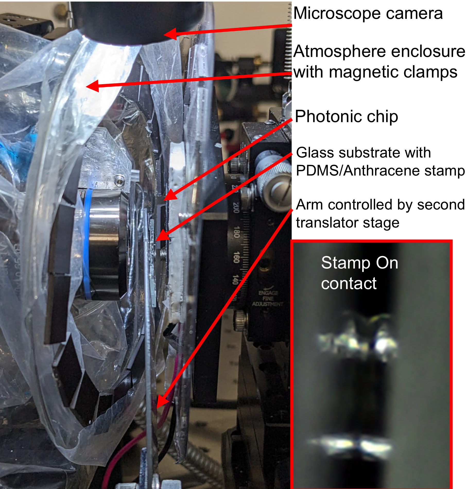
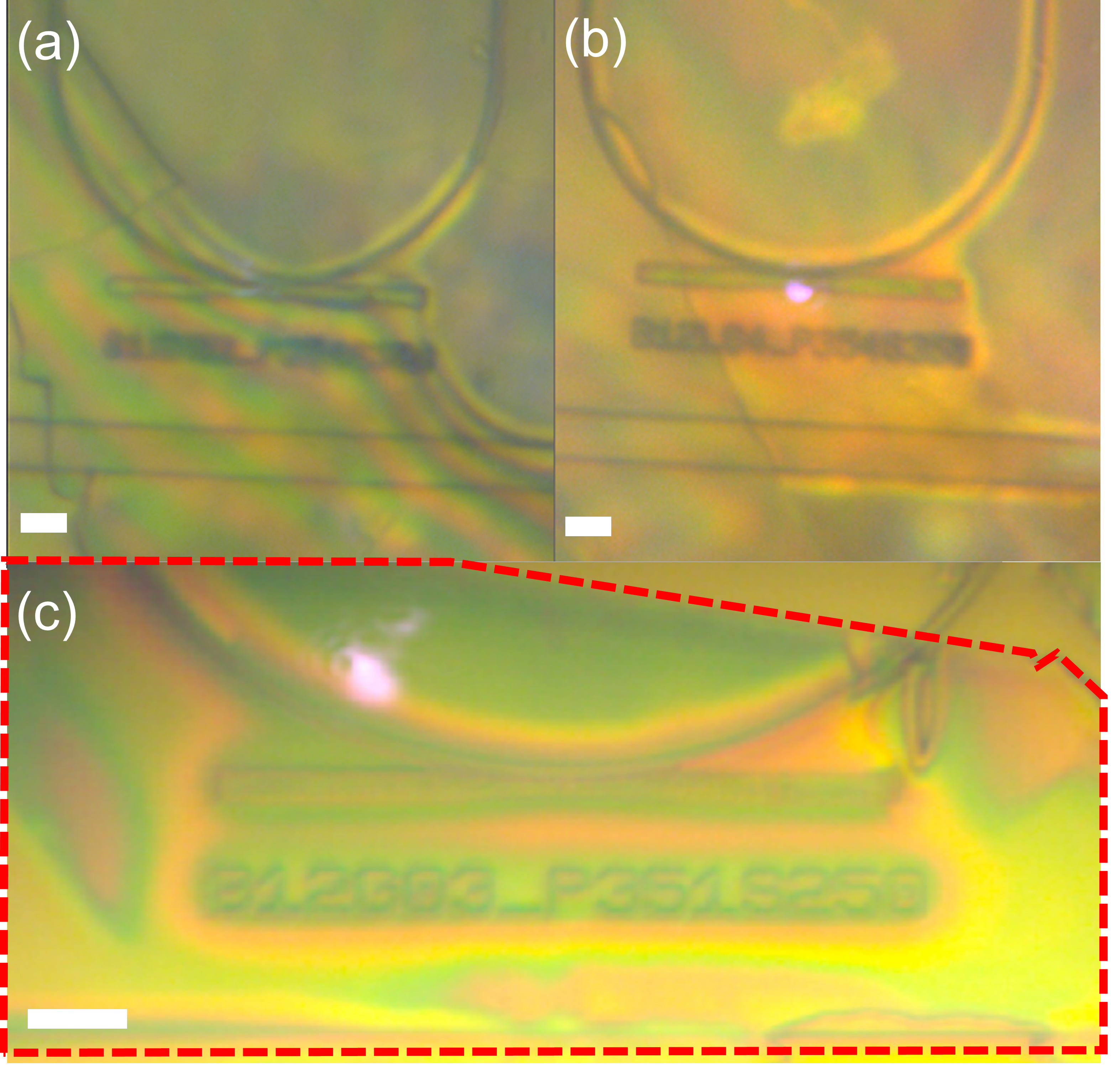
- Anthracene-assisted transfer technique: A dry-transfer method using sublimable anthracene crystals to deterministically place CNTs without contamination. "anthracene-assisted transfer technique \cite{Anthracenetechnique1Fang2023, AnthraceneTransferKeigoNaturecoms}."
- Aryl sp3 defects: Covalent aryl attachments that convert local carbon hybridization to sp3, creating exciton trapping sites in CNTs. "(6,5) CNTs with aryl sp defects are either stochastically deposited via drop-casting or deterministically positioned on photonic cavities using an anthracene-assisted transfer method guided by real-time photoluminescence monitoring."
- Cavity-enhanced emission: Increased emission at resonance due to coupling to an optical cavity mode. "Photoluminescence spectra reveal cavity-enhanced emission, while second-order autocorrelation measurements confirm single-photon propagation through the photonic integrated circuit, highlighting the potential of CNTs for scalable, room-temperature quantum photonic applications."
- Chirality (in CNTs): The (n,m) wrapping indices defining a CNT’s structure and optical transitions. "In this work, we first functionalize chirality sorted (6,5) CNTs with aryl sp defects in toluene."
- Continuous-wave mode: Laser operation with constant output power (non-pulsed). "operating at 850~nm in continuous-wave mode with 1~W excitation power."
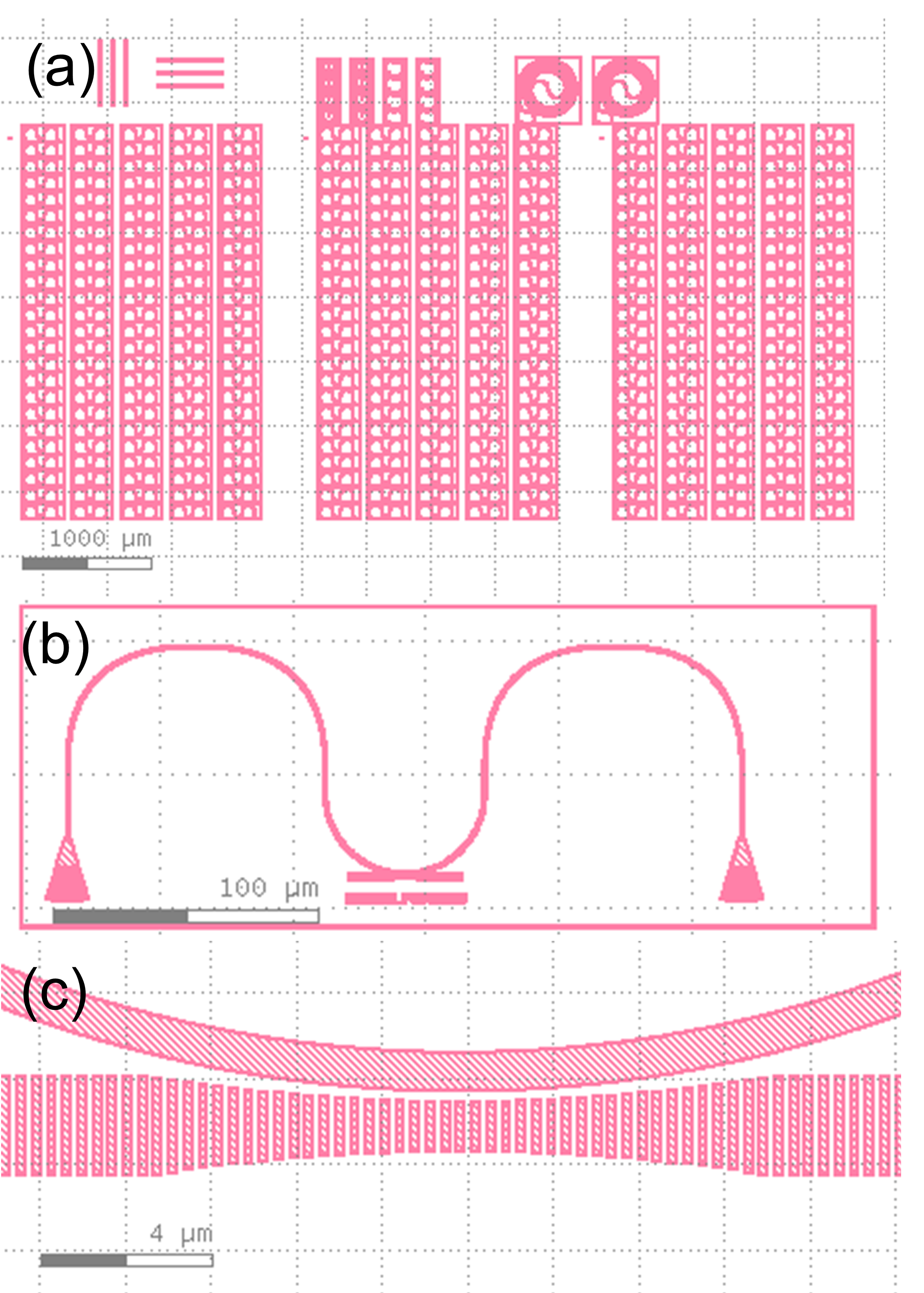
- Duty cycle (of a grating): The fraction of a grating period occupied by the ridge; controls spectral response. "The optimized cavity structures have a period of around 350~nm, a duty cycle of 0.55, and a grating width that quadratically tapers from 2.30~m to 1.15~m over a 10~m cavity length."
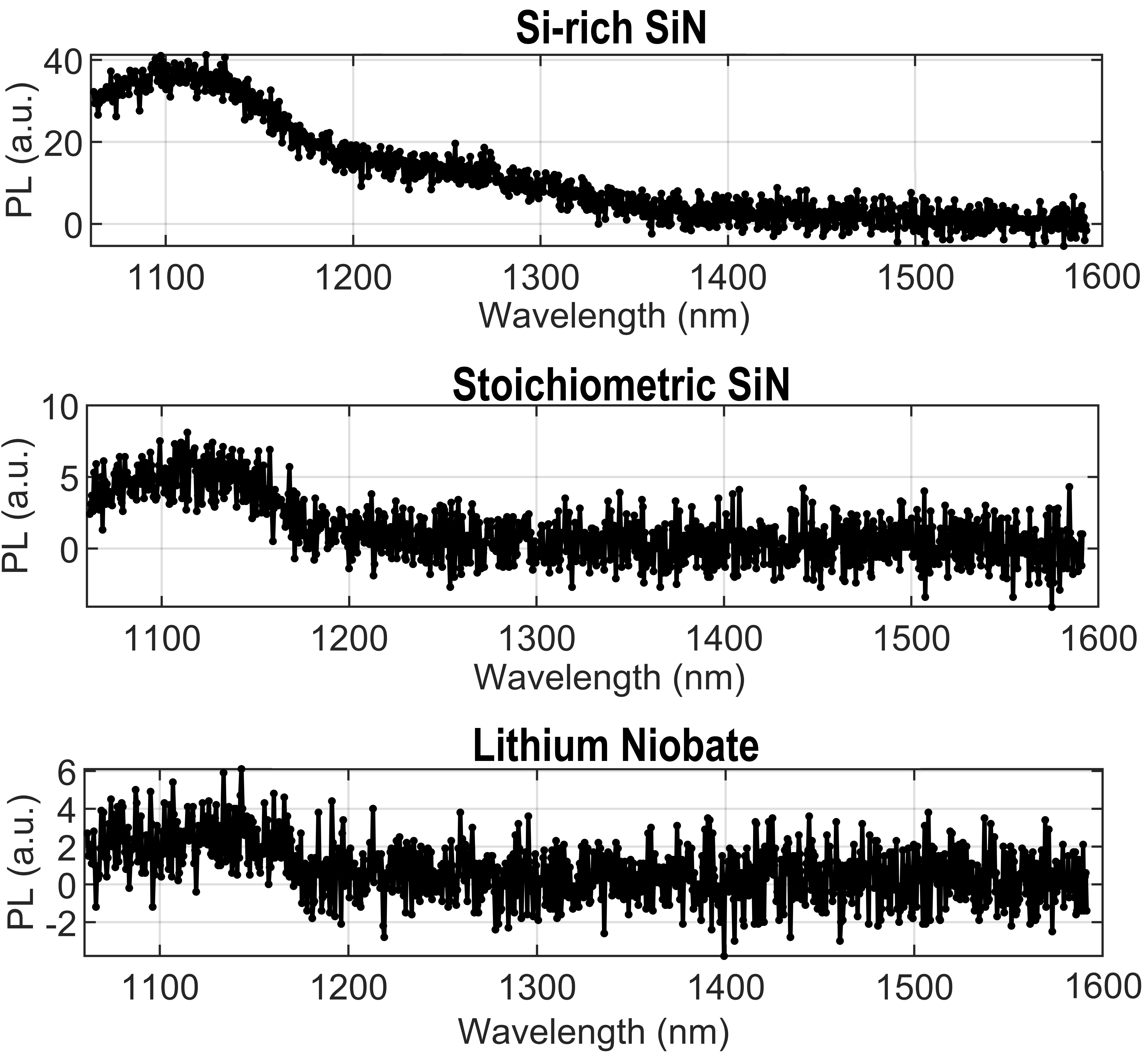
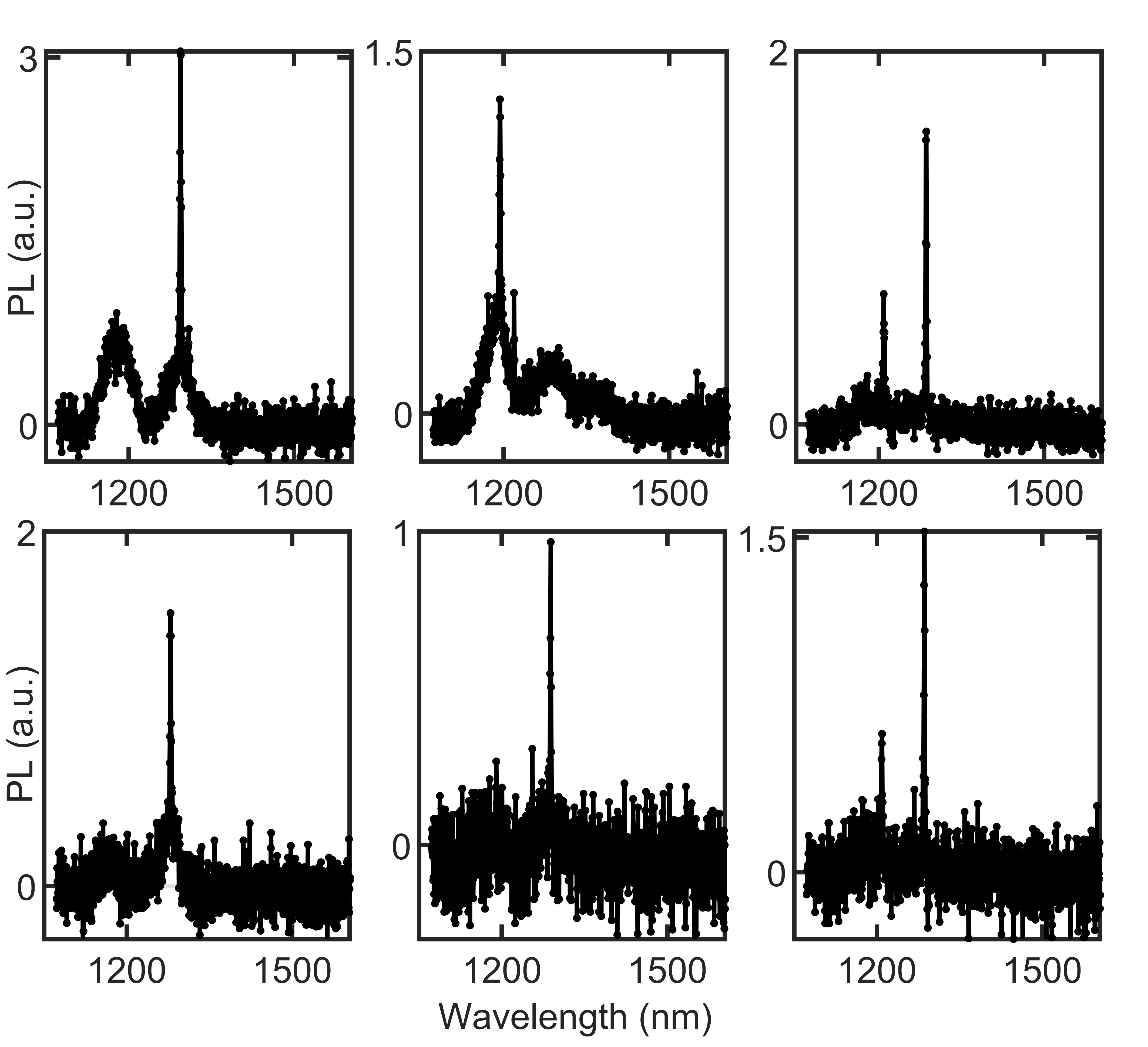
- E_{11}{*-} emission: A defect-related sub-band excitonic transition in CNTs associated with sp3 sites. "The emission peak of these functionalized CNTs is centered around 1250--1300~nm, aligning with both the transparency window of most photonic circuit materials and the primary telecommunication wavelength range that benefits from zero-dispersion optical fibers."
- Electron-beam lithography: Nanofabrication technique writing patterns with a focused electron beam. "waveguide circuits are patterned using a high-resolution Advantest F7000S-VD02 electron-beam lithography system."
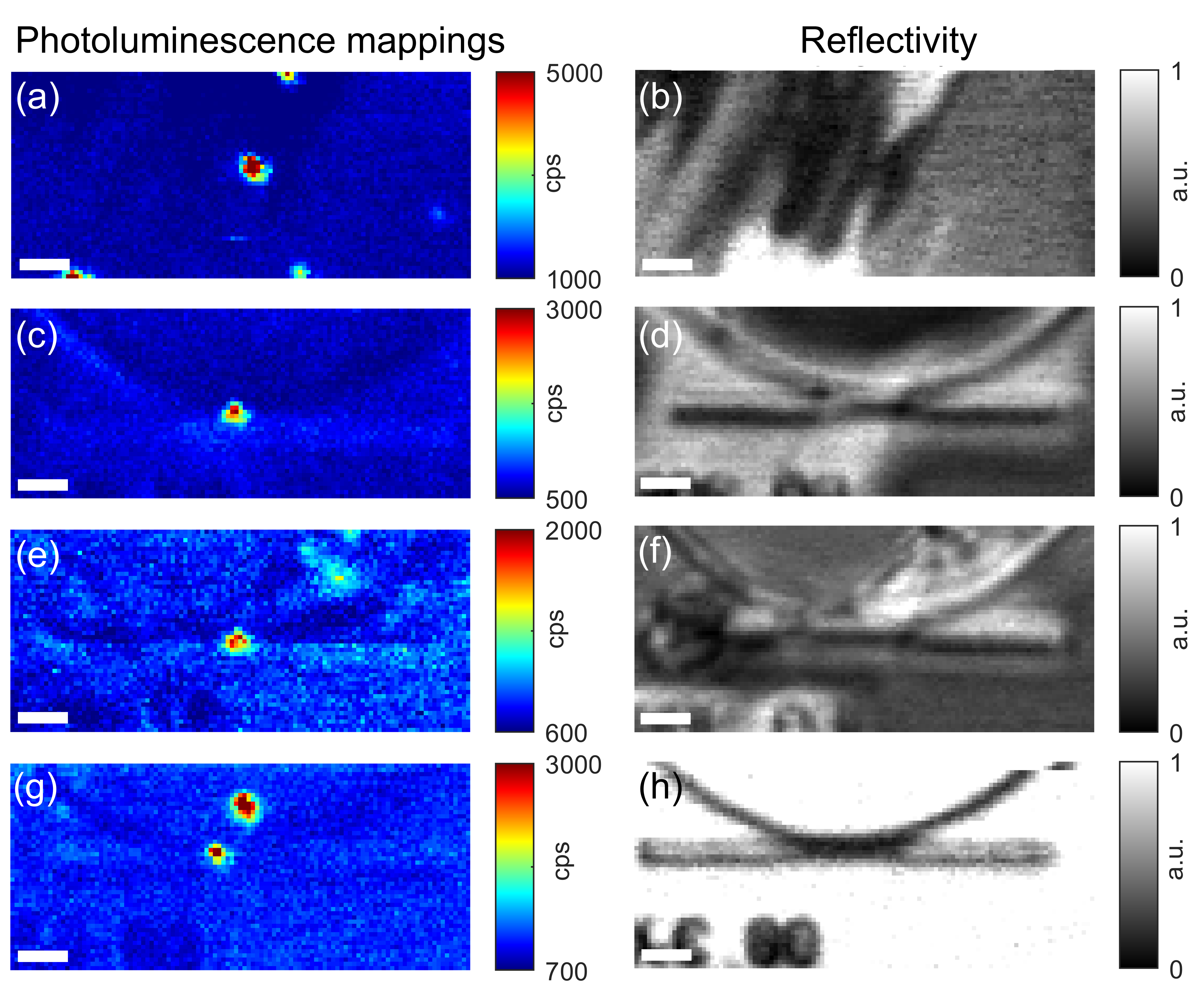
- Evanescently-coupled: Coupled via the decaying (evanescent) field between adjacent photonic structures. "By leveraging carefully designed evanescently-coupled single-mode photonic resonant cavities, the inherently broad emission spectra of CNTs are significantly narrowed to just a few nanometers."
- Exciton: A bound electron–hole pair responsible for light emission in semiconductors. "introducing exciton trapping sites through molecular defect engineering enables CNTs to emit single photons with high purity at room temperature"
- Finite-difference time-domain (FDTD): A numerical method for simulating electromagnetic fields over time. "grating photonic cavities are simulated using 2.5D finite-difference time-domain method and tailored to exhibit resonances around the CNT emission peak"
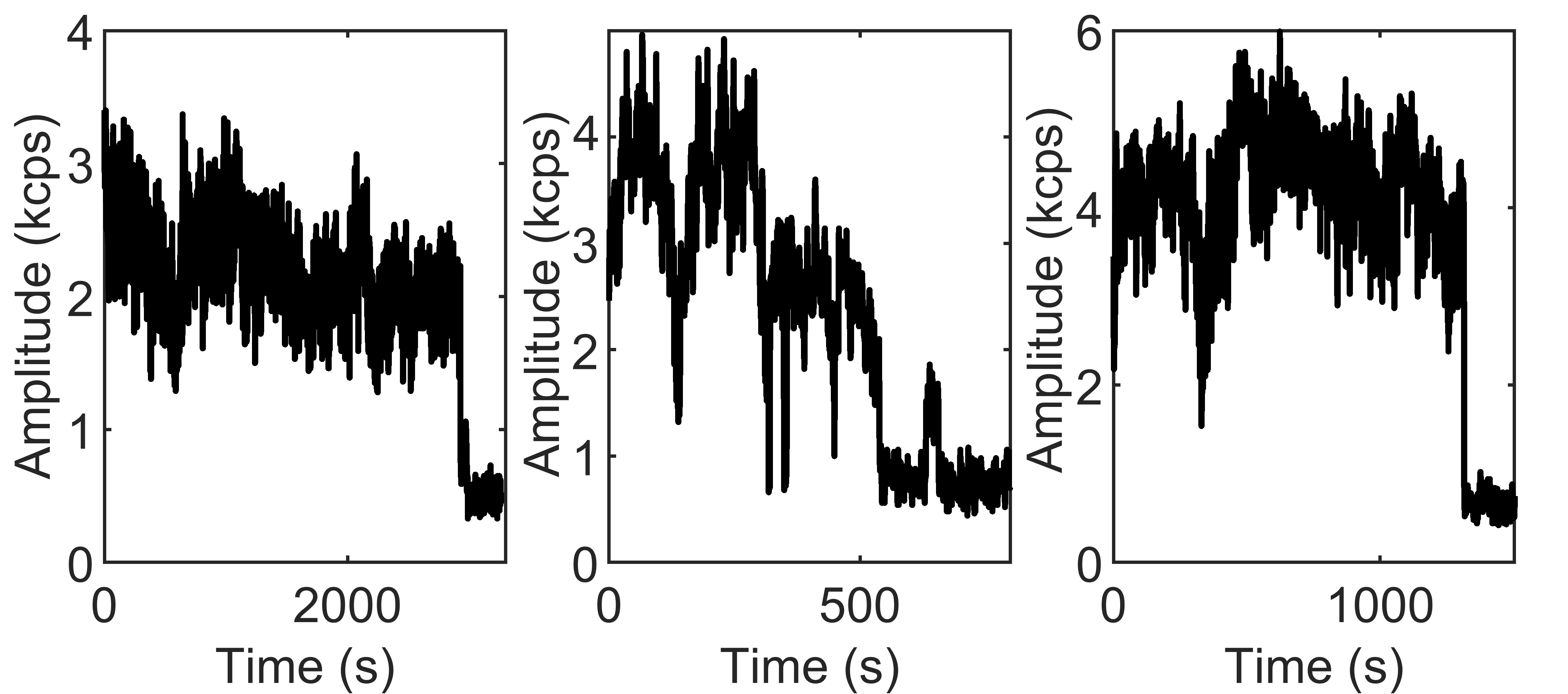
- g{(2)}(0): The zero-delay second-order correlation used to quantify single-photon purity. "Autocorrelation measurements yield values of and for the best-performing stamped and drop-cast samples"
- Grating coupler (GC): A diffractive coupler between a waveguide and an optical fiber. "Grating couplers (GCs), waveguides, and cavities are first simulated in Lumerical"
- Lithium niobate (LN): A low-loss, high electro-optic photonics platform material. "we have selected LN for the development of our circuit technology, as it offers both high optical modulation efficiency and exceptionally low emission in the near-infrared range"
- Longitudinal cavity mode: A resonance determined by the optical length along a cavity. "This relatively large cavity size is chosen to facilitate CNT coupling but leads to the appearance of a second longitudinal cavity mode"
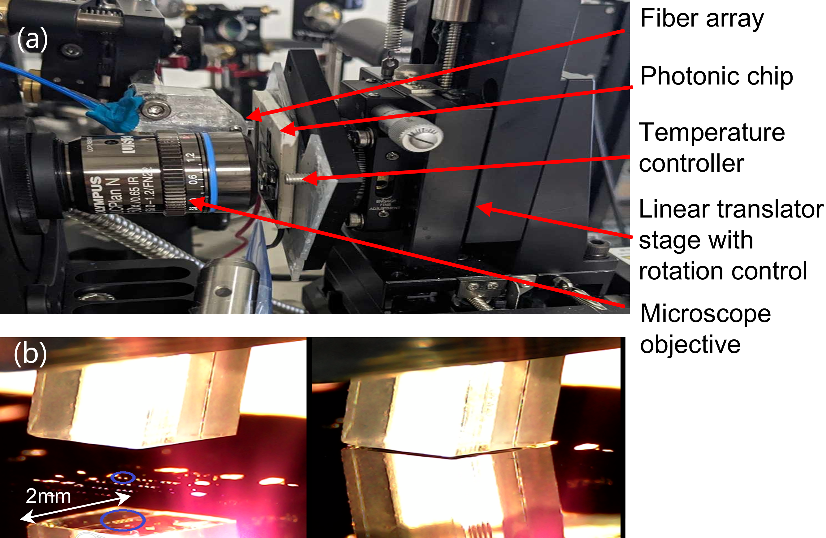
- Mode field diameter: The effective width of the optical mode in a fiber or waveguide. "Because of the large mode field diameter of the fiber and the lack of focusing optics at the output, the illuminated area on the chip is relatively wide"
- Mode-locked excitation: Pulsed laser operation with fixed repetition rate via mode locking. "the laser is switched to a 76~MHz mode-locked excitation to accelerate data acquisition"
- Mode volume: The effective spatial volume occupied by an optical cavity mode. "designed with a relatively large mode volume (1.16~, 0.52~m, where is the wavelength and is the effective refractive index)"
- Photobleaching: Irreversible loss of fluorescence/emission under illumination. "they are typically avoided due to photobleaching risks associated with prolonged pulsed excitation."
- Photoluminescence (PL): Light emission following optical excitation; used to characterize emitters. "PL measurements are then carried out using a homebuilt free-space setup comprising of optical components, a Princeton Instruments Acton 2300i spectrophotometer, and a Coherent Mira 900 laser"
- Polydimethylsiloxane (PDMS): A silicone elastomer used as a compliant stamp or substrate. "A 4500~m thick Gel-Pak polydimethylsiloxane (PDMS) sheet is first cut into a 1~mm piece"
- Purcell factor: Enhancement of spontaneous emission rate due to a resonant cavity. "The Purcell factor for broad linewidth emitters can be expressed as"
- Quality factor (Q): A measure of resonance sharpness; higher Q means lower loss. "This adjustment not only results in the clear elimination of the second mode but also leads to a slight enhancement of the resonance optical quality factor, reaching values up to 1200"
- Rib-type waveguides: Waveguides formed by partially etching a slab to leave a raised rib that guides light. "The resulting LN etch depth is measured to be 240~nm, forming rib-type waveguides."
- Single-photon emitter: A source that emits one photon at a time with antibunching. "single-walled carbon nanotubes (CNTs) have emerged as promising single-photon emitters for integrated photonics."
- Superconducting single-photon detector (SSPD): A cryogenic detector using superconducting nanowires for single-photon sensitivity. "each of the two outer FA channels is connected to a superconducting single-photon detector from Single Quantum"
- Telecom bands: Standard near-infrared wavelength ranges used in fiber-optic communications. "tunable emission across the telecom bands (1100â1600~nm) via chirality selection and defect engineering~\cite{CNTsingleemitter2}."
- Time-correlated single-photon counting (TCSPC): Technique recording photon arrival times to build timing histograms. "connected to a Qutools quTag module for time-correlated single-photon counting and event tagging."
- Transparency window: Wavelength region where a material has low absorption. "aligning with both the transparency window of most photonic circuit materials and the primary telecommunication wavelength range"
- Waveguide-coupled photonic cavity: An on-chip optical resonator coupled to a waveguide for routing emission. "single-resonant waveguide-coupled photonic cavities (Figure~\ref{fig:fig1}c), with enhanced and spectrally sharpened PL."
- Zero-dispersion optical fibers: Fibers operating near zero chromatic dispersion to minimize pulse broadening. "primary telecommunication wavelength range that benefits from zero-dispersion optical fibers."
Collections
Sign up for free to add this paper to one or more collections.