- The paper demonstrates a scalable GaP-on-diamond platform enabling deterministic SiV coupling to photonic cavities, with simulated Q factors up to 1.75×10^5 and single-shot readout fidelity exceeding 96%.
- It employs a hybrid forward and inverse design strategy to optimize the cavity’s Q/V and cooperativity while systematically quantifying intrinsic, extrinsic, and fabrication-induced losses.
- The study integrates high-yield nanofabrication, precise stamping, and spectroscopic techniques to achieve robust quantum spin initialization, with T1 exceeding 400 μs and efficient fiber-to-chip coupling.
Scalable GaP-on-Diamond Spin-Photon Interface: Nanofabrication, Integration, and Quantum Readout
Device Design and Cavity Optimization
The paper presents a fully integrated GaP-on-diamond nanophotonic platform targeting scalable spin-photon interfaces with deterministic single-defect (SiV center) coupling for quantum information applications. The core device is a GaP photonic crystal (PhC) nanobeam cavity, optimized for strong evanescent coupling to silicon-vacancy (SiV) centers implanted shallowly into the underlying diamond substrate.
Key elements of the cavity optimization include:
- Quadratic chirping of the lattice constant to localize the optical mode (minimizing V and maximizing Q) while preserving significant overlap with SiV dipoles positioned ≈20 nm below the interface.
- Hybrid design combining forward-design (maximizing Q/V) and inverse design via global (LIPO) and local (trust-region) search methods to directly maximize the expected cooperativity C, which encapsulates the Purcell enhancement and spatial overlap with the emitter.
- Separation of loss contributions into intrinsic radiative loss, extrinsic waveguide-coupling, and fabrication-induced losses, allowing a systematic quantification of experimentally achievable performance.
Evaluation of the objective function for the optimized design yields simulated Qi=1.75×10⁵, V=1.86(λ/n)3, and field overlap ∣Ey(xa)/max∣E∣∣2=0.25. For a realistic fabrication-constrained Qfab=5×10⁴, the lower-bound cooperativity is C=23 (vs. C=102 for ideal fabrication), confirming strong potential for the system to operate in high-cooperativity (and thus high-fidelity spin-photon interface) regimes.
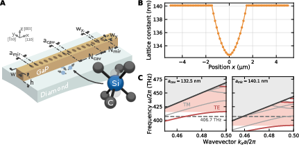
Figure 1: Nanobeam cavity design: (A) device cross-section with parameter labels; (B) optimized lattice constant profile; (C) simulated band structures illustrating midgap resonance and photonic bandgap contrast.
Fabrication, Stamping, and Integration Protocol
The integration platform exploits a heterogeneously fabricated GaP nanophotonic cavity that is transferred onto a planar diamond chip hosting a shallow ensemble of SiV centers. The process entails:
- EBL patterning of etched GaP-on-AlGaP membranes to define the PhC cavity arrays and embedding frames for mechanical support throughout the process.
- Controlled undercut and critical-point drying to release free-standing nanodevices.
- Polymer stamp transfer using a PC/PDMS composite, leveraging temperature-driven PC melt to pick and deterministically align hundreds of devices onto defined regions of the cleaned diamond chip.
Post-stamping, the PC film is dissolved, leaving the nanophotonic devices atop the SiV-rich diamond surface with >99% yield.
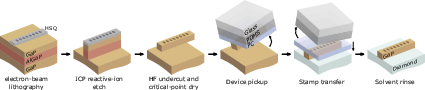
Figure 2: Overview of the GaP nanobeam device fabrication flow, from EBL and etch through release and final transfer to diamond.
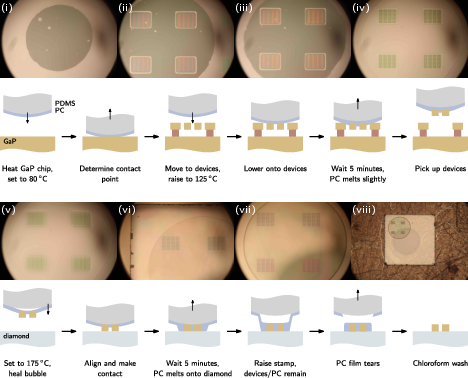
Figure 3: Stamping sequence: sequential optical micrographs document device pickup, alignment, transfer, and release onto the diamond host.
Nanophotonic Coupling and Excitation
Efficient fiber-to-chip and chip-to-free-space coupling is critical for high-throughput device metrology and scalable photonic interconnects.
- Elliptical free-space grating couplers are co-designed with the PhC cavities, providing broadband transmission (≈20%) into a narrow angular profile, facilitating both excitation and collection via high-NA objectives.
- SEM and FDTD characterization validate the uniformity and spectral fidelity of the gratings. The primary bottleneck in system efficiency is traced to the grating’s numerical aperture-collection mismatch.
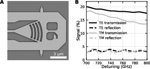
Figure 4: (A) SEM of elliptical grating; (B) FDTD-modeled broadband TE/TM reflection and transmission showing dominant TE-mode coupling.
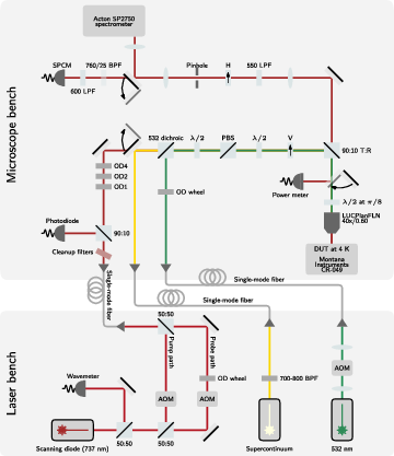
Figure 5: Schematic of the integrated cryogenic microscope: laser, DAQ, and detector submodules enabling high-resolution, resonant, and off-resonant measurements.
Spectroscopic Characterization and Gas Tuning
To match device resonances to specific SiV transitions, xenon gas condensation is used to controllably redshift cavity modes, achieving reliable spectral overlap.
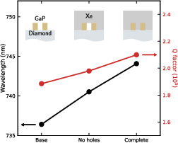
Figure 6: Resonance tuning and Q versus xenon load: maximal shift is observed when PC holes fill, but is limited by cryostat geometry.
Transmission spectra are acquired both in broadband (supercontinuum) and narrowband (scanning diode laser, with high-precision wavemeters) regimes. Lorentzian fits to broadband spectra extract cavity Q and spectral homogeneity metrics, while narrowband scans precisely resolve emitter-cavity interactions and allow evaluation of dipole-induced transparency (DIT).
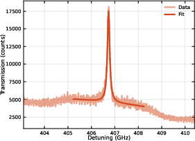
Figure 7: Example broadband transmission measurement: Lorentzian fit isolates TE cavity response atop TM and background contributions.
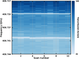
Figure 8: Multiple high-resolution DIT scans show dual high-contrast dips for SiVs coupled to a single cavity, enabling direct extraction of coupling rates.
Experimental Results: High-Cooperativity Spin-Photon Coupling
Multiple device instances are characterized for quantum emitter-cavity coupling:
- DIT features are robustly observed in both “drop” and “thru” geometries, with contrasts dependent on design and coupling configuration.
- Quality factors of Q∼3000−10000 are measured post-integration.
- Lower bounds on single-emitter cooperativity range from C>0.36±0.01 to C>0.50±0.02, with all values suppressed by residual spin and orbital thermalization. These values approach or surpass state-of-the-art for hybrid photonic/dipole platforms, confirming strong-coupling regime accessibility.
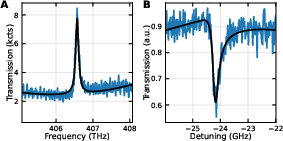
Figure 9: Transmission (broadband and DIT) for a drop-coupled device with Q=4300; lower-bound C>0.50 from input-output model fit.
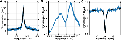
Figure 10: Single-peak DIT for drop-coupled device with Q=2900 and C>0.36.
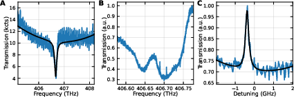
Figure 11: Thru-coupled device: Q=4200, two resolved DIT dips; fit constraints provide C>0.45 lower bound.
Spin Initialisation, Relaxation, and Optical Quantum Readout
A custom magnetic mount aligns the external field to selected SiV principal axes, stabilizing the spin basis for optical pumping and readout. Fine-tuning of field angle and strength is corroborated by modeling and experimental transition splittings.
- Spin relaxation T1 is quantified in both misaligned (α∼70∘) and near-aligned (α≲4∘) field configurations. In the optimal geometry, T1 exceeds 400 μs—a value limited predominantly by magnetic field alignment and local defect environment, and in agreement with prior reports on SiV spin-lattice relaxation.
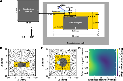
Figure 12: 3D simulation and experimental schematics for the embedded SmCo magnetic mount and field-control protocols.
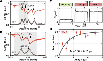
Figure 13: Off-axis field experimental signatures: combined PLE and DIT, selective ionization, optical pumping and spin-recovery kinetics.
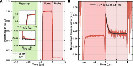
Figure 14: Optical switching via resonant spin pumping and DIT recovery readout decays.
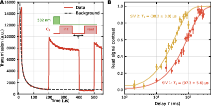
Figure 15: Spin-pumping and T1 decay for near-aligned field; robust two-level thermalization behavior.
Single-shot measurements are demonstrated, extracting spin-projected quantum-jumps in transmission, resulting in a single-shot readout fidelity F=96.0±0.3\% for optimal thresholds, and confirming quantum non-demolition readout capability in the GaP-on-diamond photonic platform.
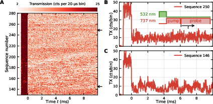
Figure 16: Raw time-resolved single-shot transmission, revealing quantum jumps, photon shot-noise, and blinking events.
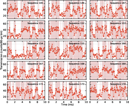
Figure 17: Post-selected sequences: clear thresholding allows for >96% single-shot spin state discrimination.
Implications, Comparisons, and Outlook
By integrating deterministic, high-yield GaP nanocavity arrays directly onto high-purity diamond chips, this work achieves a substantial advance in scalable, hybrid quantum photonics. The achieved cooperativities and spin T1 reservoirs closely match, or exceed, leading integrated quantum node demonstrations across SiV and related group IV color centers [Sipahigil et al., Science 2016; Evans et al., Science 2018]. The methodology's high device yield, field-insensitive fabrication, and post-transfer tuning pipelines support wafer-scale scaling, critical for multiplexed quantum repeater networks and distributed quantum memory arrays.
Several open avenues are noted:
- Further Q enhancement: leveraging state-of-the-art lithographic and etch optimization, as well as surface passivation, should bridge the remaining gap to the Qi≳105 regime required for error-corrected network nodes and entanglement distribution [Bhaskar et al., Nature 2020; Stas et al., Science 2022].
- Full integration: coupling to waveguide buses and on-chip switching elements is compatible with the presented architecture, informed by recent advances in CMOS backend hybrid photonic integration [Li et al., Nature 2024], telecommunication-wavelength quantum networking [Bersin et al., PRX Quantum 2024], and hybrid quantum interconnects [Riedel et al., (Riedel et al., 8 Aug 2025)].
- Spin-photon interface expansion: the method is generalizable to alternative emitters (SnV, NV, rare-earth doped) and other wide-bandgap photonic platforms, as well as to composite functionalities such as non-reciprocity, acousto-optic tuning, and parametric processes enabled by the nonlinear properties of GaP [Wilson et al., Nat. Photonics 2020].
Conclusion
This work establishes gallium-phosphide-on-diamond nanophotonic cavities as a powerful, deterministic, and scalable spin-photon interface platform. The approach combines optimal cavity performance, robust fabrication and transfer, efficient optical access, and direct quantum state readout. These results define a high-cooperativity, high-fidelity standard for hybrid quantum node integration, bridging fundamental color center quantum optics, scalable photonic engineering, and quantum network deployments (2601.04733).