Design and Operation of Wafer-Scale Packages Containing >500 Superconducting Qubits
Abstract: Packages capable of supporting large arrays of high-coherence superconducting qubits are vital for the realisation of fault-tolerant quantum computers and the necessary high-throughput metrology required to optimise fabrication and manufacturing processes. We present a wafer-scale packaging architecture supporting over 500 qubits on a single 3-inch die. The package is engineered to suppress parasitic RF modes, and to mitigate material loss through simulation-informed design while managing differential thermal contraction to ensure robust operation at millikelvin temperatures. System-level heat-load calculations from a large wiring payload show this package may be operated in commercial dilution refrigerators. Measurements of the qubits loaded into the package show median $T_1$, $T_{2e} \sim 100~μ$s ($\sim$100 qubits) alongside readout with median fidelity of 97.5% (54 qubits) and a median qubit temperature of 36 mK (54 qubits). These results validate the performance of these packages and demonstrate that large-scale integration can be achieved without compromising device performance. Finally, we highlight the utility of these packages as a tool for high throughput feedback on qubit figures of merit over large sample sizes, allowing identification of performance outliers in the tails of the coherence distribution, a critical capability for informing fabrication and manufacture of high-quality quantum qubits and quantum processors.
Paper Prompts
Sign up for free to create and run prompts on this paper using GPT-5.
Top Community Prompts
Explain it Like I'm 14
Overview: What this paper is about
This paper explains how to build and use a “wafer-scale” package that can hold and measure more than 500 superconducting qubits on a single large chip (about the size of a small pizza slice, 3 inches across). Superconducting qubits are tiny circuits that behave according to quantum rules when cooled to near absolute zero. The package is designed to protect these qubits from noise, keep them very cold, connect them to measurement equipment, and still let them perform well. The team also shows how this setup helps them quickly test lots of qubits at once, which is crucial for making better, larger quantum computers in the future.
The main goals in simple terms
- Build a big, reliable “home” for hundreds of qubits on one chip that:
- Blocks unwanted microwave “echoes” inside the box that would disturb the qubits.
- Minimizes energy losses from the materials used in the box.
- Stays aligned and intact when cooled from room temperature down to a few thousandths of a degree above absolute zero.
- Can be run inside standard ultra-cold freezers used by researchers.
- Prove the package works by measuring over 100 qubits and checking:
- How long they remember information (their “coherence time”).
- How accurately they can be read out (readout fidelity).
- How cold the qubits really are (their effective temperature).
- Show how testing lots of qubits at once gives trustworthy statistics that help improve manufacturing.
How they did it: Methods explained in everyday language
The package design
Think of the package as a quiet, well-insulated concert hall for delicate instruments (the qubits). It has:
- A metal lid and base that shield the chip from outside noise.
- A custom circuit board (PCB) underneath that connects to the qubits for control and measurement.
- A thin spacer that sets the distance between the qubits and the PCB pins.
- Dozens of microwave cables coming in from outside to talk to many qubits through shared lines.
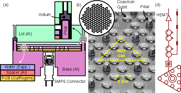
The qubits are “coaxmon transmons” — a common kind of superconducting qubit — and each qubit has a partner “readout resonator” that works like a tiny radio tuned to a specific frequency. Several of these resonators share a single readout line using “frequency multiplexing,” similar to how many radio stations share the airwaves without interfering if they use different frequencies.
A special “Purcell filter” on the PCB acts like a one-way door: it lets measurement signals through to the resonators but helps block unwanted energy from leaking out of the qubits.
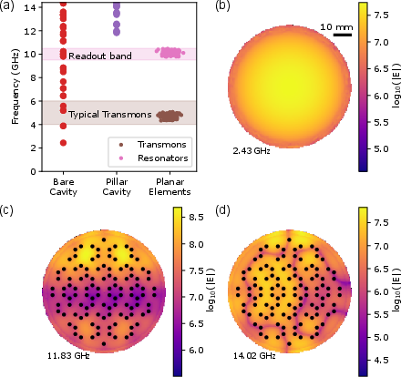
Taming microwave echoes (“box modes”)
Big metal boxes can ring like a drum at certain microwave tones, called “box modes.” These echoes can cause qubits to lose energy faster or interfere with measurements. To fix that, the team filled the space with metal pillars that connect the lid and base. These pillars act like a forest of posts that break up the echoes and push them to much higher frequencies where they don’t bother the qubits or their readout signals.
Keeping things aligned when very cold
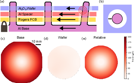
Materials shrink when cooled. Different materials shrink by different amounts. The team simulated this “thermal contraction” to make sure:
- The chip wouldn’t bump into the pillars when it shrinks.
- The PCB pins would still line up with the qubits. They added careful gaps around the pillars and chose materials to avoid collisions or misalignment.
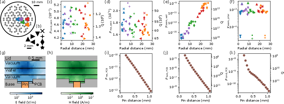
Estimating and reducing losses
Any loss (like friction for electricity or tiny absorbing layers) can reduce qubit performance. The team used computer simulations (finite element analysis) to estimate how much energy from a qubit’s electric and magnetic fields can leak into:
- The package walls (metal losses),
- Thin surface layers (dielectric losses, like tiny insulating coatings),
- Joints between different pieces (seam losses),
- The PCB materials.
They found the package adds very little loss compared to what the qubits already have from their own materials. In other words, the packaging likely won’t be the bottleneck.
Making sure the ultra-cold fridge can handle it
Quantum computers sit in special freezers called dilution refrigerators. The team calculated the total heat load from all the cables and signals needed to fully wire this big package. Their numbers show it should work fine inside standard commercial fridges, even when everything is connected, and leave plenty of cooling power to spare.
How they measured the qubits
- They tested 105 qubits using shared readout lines, without individual control lines for each qubit. Instead, they cleverly sent both drive and readout signals through the same path, using the filter to keep qubit energy loss low.
- They automated calibration so many qubits could be tuned and measured efficiently.
- They optimized readout settings and recorded lots of measurement shots to estimate errors and effective temperatures.
- They repeated coherence measurements many times per qubit to get reliable “median” values.
What they found and why it matters
- Scale: The package supports over 500 qubits on one 3-inch die.
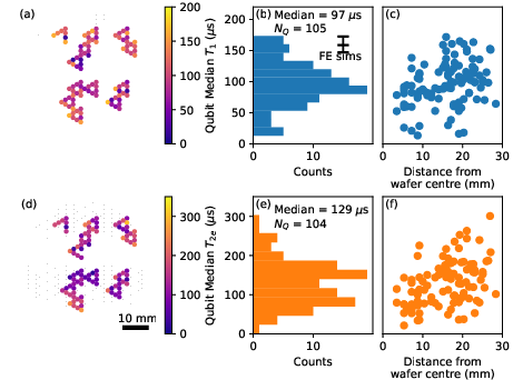
- Coherence: Across roughly 100 qubits, the typical memory times were about 100 microseconds for both T1 (energy loss time) and T2e (dephasing time). For context, a microsecond is a millionth of a second — in the quantum world, 100 microseconds is good and usable.
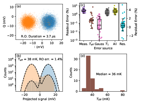
- Readout accuracy: For 54 qubits, the typical readout fidelity was about 97.5% (2.5% error). Most of this error came from qubits relaxing during the relatively long readout pulse, not from the package itself. This can be improved with faster readout and better amplifiers.
- Temperature: The qubits were very cold, with a typical effective temperature of about 36 millikelvin (that’s 0.036 degrees above absolute zero), which is excellent for “passive reset” (just waiting for the qubit to relax).
- Packaging losses are small: Simulations and measurements agree that the package is not what limits qubit performance; the chip’s own materials are the main factor. This is good news, because it means the package can scale without harming the qubits.
- Strong, low-loss joints: They set a lower bound (a safe minimum estimate) on the electrical quality of the aluminum–indium joints that connect pillars to the lid. These joints look sufficiently low-loss for good performance.
- Fridge compatibility: With all the planned wiring and signals, the calculated heat load is well within what typical commercial dilution refrigerators can handle.
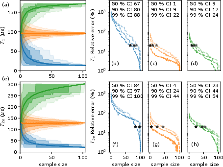
- Big-data advantage: By measuring many qubits, they showed that:
- You can estimate the “typical” performance (the median) with relatively few qubits.
- But to reliably find the very best or the very worst qubits (the extremes), you need to measure many more. This is essential for improving manufacturing, because the worst devices can limit overall system performance.
What this means for the future
This work shows a practical path to larger quantum processors:
- The package can host hundreds of qubits without hurting their performance.
- It is compatible with standard ultra-cold hardware.
- It enables high-throughput testing — measuring many qubits quickly — giving manufacturers the data they need to spot problems and improve their processes.
- With straightforward upgrades (like adding per-qubit control lines and low-noise parametric amplifiers), the same architecture can serve as a powerful readout module inside a full quantum processor.
In short, this package helps bridge the gap between small lab experiments and the much bigger, more reliable quantum machines needed for fault-tolerant quantum computing.
Knowledge Gaps
Below is a concise, actionable list of unresolved knowledge gaps, limitations, and open questions identified in the paper. Each point is framed to guide concrete follow‑up work.
- Full‑scale operation not demonstrated: Performance, stability, and cross‑talk when all 56 multiplexed cells and >500 qubits are simultaneously wired and operated remain untested (e.g., frequency‑collision rates, resonator crowding, readout intermodulation, HEMT dynamic range, and acquisition throughput limits).
pipeline).
- Simultaneous multiplexed readout scaling: Quantify readout cross‑talk and intermodulation distortion when reading nine resonators per cell concurrently across 56 lines; characterize amplifier compression and isolation requirements (circulators/isolators) under worst‑case aggregate power.
- Control architecture gap: Per‑qubit XY control is omitted; the feasibility, thermal load, wiring density, box‑mode impact, and cross‑talk of integrating 500+ dedicated control lines into the lid are not validated experimentally.
- Gate performance not evaluated: No single‑qubit (RB/CRB) or two‑qubit gate error benchmarks are reported using the current “readout‑port driving” approach or the proposed per‑qubit XY wiring, leaving gate fidelity, cross‑talk, and calibration stability unquantified.
- PCB‑based Purcell filter characterization: The 10 GHz PCB filter performance at millikelvin temperatures (S‑parameters, passband variation across 56 cells, Qext spread, temperature/frequency drift, lot‑to‑lot reproducibility) is not measured in situ; only simulations are referenced.
- Readout optimization trade‑offs: The targeted coupling/Qext vs. T1‑limited readout error trade‑off is not systematically mapped (e.g., dependence on pin height, resonator linewidth, drive power), and the impact on measurement‑induced transitions is not quantified.
- Parametric amplifier integration: Mechanical, thermal, and electromagnetic integration of JPAs/JPCs (pump leakage, isolation, dynamic range, stability, added noise) is not demonstrated; effect on readout speed and fidelity distribution across 500+ channels remains open.
- Box‑mode mitigation experimentally unverified: While simulations show pillar arrays push modes >~12 GHz, there is no experimental verification (e.g., cavity S‑parameter mapping, qubit T1 vs. frequency sweeps, tone‑probe spectroscopy) to confirm mode frequencies/Qs and suppression margins with the fully assembled package.
- Pillar lattice optimization: How pillar geometry, pitch, and placement scale to larger wafers (4–6 inch) and different die layouts to keep all box modes outside qubit/readout bands is not studied; tolerance to machining/assembly misalignment is unknown.
- Packaging‑loss budget validation: Simulations suggest negligible packaging loss, but experimental deconvolution is missing (e.g., varying pin distance in a controlled study and correlating with T1; swapping PCB materials; before/after surface treatments).
- Unquantified PCB cryo loss parameters: Loss due to PCB metal oxides and seams at millikelvin temperatures is omitted for lack of literature values; dedicated coupon measurements (e.g., CPW resonators on Rogers at mK, silver‑oxide surface resistance) are needed to close the model.
- Aluminum 5083 RF properties: The superconducting RF surface resistance and penetration depth of Al‑5083 at 4–10 GHz and mK are not measured; impact of alloy composition, surface roughness, and treatments (e.g., polish, passivation) remains uncertain.
- Indium–aluminum seam reliability: Only a weak lower bound on seam conductance is inferred via qubit T1; direct seam‑loss measurements (e.g., cavity ring‑down test structures), intermetallic formation analysis, and aging/thermal‑cycling reliability studies are needed.
- Mechanical/thermal robustness: Differential contraction modeling is presented, but empirical data on alignment drift, wafer yield, pillar/wafer damage, and performance changes over many thermal cycles are not provided.
- Thermal‑load model unvalidated: The fully wired thermal model (504 XY, 56 readout, 56 pump lines) is not experimentally validated; actual MXC load, stage temperatures, and stability under continuous operation and increased cadence (active reset) are untested.
- Magnetic environment and vortices: The shield’s >20 dB attenuation is not tied to measured residual on‑chip fields; susceptibility to flux trapping in large Al structures, cooldown protocols, and their impact on coherence/noise are unexplored.
- Radiative and quasiparticle environment: The efficacy of the “hybrid filters” and light‑tight can in suppressing infrared/UV pair‑breaking radiation is not quantified (e.g., QP density measurements, poisoned‑event rates, correlation to T1/T2e variability).
- Effective temperature inference: Qubit temperature is inferred solely from readout histograms; independent validation (e.g., up‑transition rate measurements, detailed SPAM error budget, resonator‑photon population) is not provided.
- Dephasing analysis gap: Only T2e is reported; T2* distributions, noise spectra, and identification of dominant dephasing mechanisms (e.g., photon shot noise, 1/f charge/flux noise, packaging‑induced photon population) are absent.
- Crosstalk quantification: Drive and measurement cross‑talk (both within a 9‑1 cell and across neighboring cells), Stark shifts from shared lines, and measurement‑induced dephasing of adjacent qubits are not quantified experimentally.
- Frequency planning and yield: Population‑level distributions of qubit and resonator frequencies across the wafer (collision rates, fabrication spread) are not shown; strategies for frequency assignment and yield optimization are not discussed.
- Multi‑wafer/process variability: All statistics are from a single wafer; between‑wafer/process‑run variability and packaging‑to‑packaging reproducibility are not assessed, limiting generality of the bootstrapping conclusions.
- Outlier root‑cause analysis: While tails of the T1/T2e distribution are highlighted as important, no correlation analysis with fabrication metadata (e.g., location, lithography, etch, surface morphology), proximity to pillars/walls, or resonator parameters is provided.
- Two‑qubit integration path: The packaging’s compatibility with couplers/bus resonators, wiring for tunable couplers, and impact on crosstalk/box modes is not addressed; no plan for scalable entangling gate routing is detailed.
- Vibration and microphonics: Sensitivity of large 3D assemblies (lid/base/pillars) and PCB/readout resonators to fridge vibrations and microphonics (phase noise, readout stability) is not measured.
- Connectorization and reliability: The SMPS/coax interfaces’ thermalization, lifetime at mK, insertion loss spread, and mechanical reliability under repeated cycles are not characterized.
- Readout Qext uniformity: The distribution and spatial dependence of Qext and measurement efficiency across the wafer (due to pin‑height tolerances, alignment, PCB variation) are not reported; contribution to readout‑fidelity spread is unknown.
- Calibration and orchestration at scale: The automation strategy scales to ~100 qubits but not to 500+; scheduling, resource contention, and time‑to‑calibrate for full devices, along with failure‑mode handling, are not detailed.
- Comparison to alternatives: No quantitative comparison to other wafer‑scale or 3D packaging (e.g., pogo pins, through‑silicon‑vias, flip‑chip with interposers) is provided to clarify trade‑offs in loss, scalability, thermal load, and assembly complexity.
- Generalization beyond 3″ wafers: Mechanical, electromagnetic, and thermal implications of moving to 4″–6″ wafers (pillar lattices, mode spectra, tolerances, yield) are unaddressed.
- On‑chip vs off‑chip filter co‑design: The interplay of PCB filters with potential on‑chip filters or multiplexers (for faster readout and stronger Purcell suppression) is not explored; co‑design rules and stability margins are missing.
- Environmental aging: Long‑term stability (months–years) of indium joints, aluminum surfaces, and PCB materials at mK, including creep, interdiffusion, and oxidation under repeated thermal cycling, is not studied.
Practical Applications
Immediate Applications
The following items can be deployed now, using the paper’s demonstrated package, methods, and measurement workflows.
- Wafer-scale high-throughput qubit metrology for fabrication optimization
- Sectors: hardware manufacturing, semiconductor/quantum foundries, academia (materials/process research)
- Use case: characterize >100 qubits per wafer in a single cooldown to quantify median, tails (min/max), and spatial variability of T1/T2e; feed results back to lithography, etch, deposition, and cleaning recipes
- Tools/products/workflows: wafer-scale package (>500 qubits), 9-1 PCB multiplexed readout lines, QBlox control hardware, automated calibration batches, bootstrapped statistics to determine required sample sizes for QA
- Assumptions/dependencies: access to a commercial dilution refrigerator; availability of basic RF instrumentation; qubit designs compatible with coaxmon/transmon-style readout; omission of per-qubit drive lines acceptable for metrology runs
- Packaging playbook to suppress parasitic box modes using machined pillar “metamaterial” cavities
- Sectors: quantum hardware engineering, instrumentation, academia
- Use case: redesign enclosures to push cavity modes above 10–12 GHz, reducing Purcell decay, crosstalk, and measurement-induced dephasing for transmons and similar devices
- Tools/products/workflows: aluminum lid/base with pillar array through wafer apertures; EM simulation of cavity modes; mechanical design guidelines for pillar placement
- Assumptions/dependencies: precise machining and wafer aperture alignment; mode suppression depends on pillar geometry and grounding continuity
- PCB-based 9-1 multiplexed Purcell-filter readout modules
- Sectors: cryogenic instrumentation, test equipment vendors
- Use case: reduce coaxial cable count and simplify wiring while maintaining radiative decay suppression and enabling readout/control via shared lines
- Tools/products/workflows: multi-layer Rogers PCB triangular filters centered ~10 GHz with Lorentzian response; capacitive coupling across a spacer-defined vacuum gap; one-port combined control and readout per cell
- Assumptions/dependencies: acceptable drive power through single-stage filter for Rabi; filter bandwidth alignment to resonator frequencies; Qext tuned via pin distance
- Thermal load budgeting for cryostat integration with commercial dilution refrigerators
- Sectors: cryogenics, facilities planning, data center infrastructure for quantum
- Use case: verify payloads (e.g., 504 attenuated drive lines, 56 readout chains, 56 pump lines) meet MXC stage limits; plan for ~3 μW loads at 20 mK with sufficient margin
- Tools/products/workflows: stage-by-stage heat-load calculators (per Krinner et al. and Manifold et al.), wiring budgets, amplifier placement strategies
- Assumptions/dependencies: conservative continuous-wave drive assumptions (e.g., −64 to −78 dBm/qubit), pump powers ~−60 dBm, measured cooling power (25–30 μW at 20 mK)
- Readout error budgeting and optimization workflow
- Sectors: software/instrumentation for quantum control; lab operations
- Use case: improve readout fidelity by identifying dominant contributors (T1 decay during measurement, finite temperature, Gaussian overlap) and tuning pulse amplitude/frequency/duration
- Tools/products/workflows: IQ Gaussian modeling, passive reset, measurement duration optimization; option to add shelving or driven reset for further reductions
- Assumptions/dependencies: present configuration is HEMT-first (no paramps); measurement durations median ~6.2 μs; T1 fluctuations over time must be tracked
- Statistical sampling protocol to set QA acceptance criteria for wafer lots
- Sectors: manufacturing quality control, procurement, policy within organizations
- Use case: use bootstrapping to determine how many qubits to measure to estimate median vs tails (min/max) within specified confidence intervals; define lot acceptance by distributions, not only single best value
- Tools/products/workflows: bootstrapped confidence intervals; sampling plans (e.g., 5–20 qubits for medians vs ~50% of wafer for minima at 20% error in 50% CI)
- Assumptions/dependencies: measured ensemble is representative; temporal stability comparable to reported fluctuations; consistent measurement protocol
- Process window and assembly guidance for low-loss seams (Al/In joints)
- Sectors: mechanical/assembly engineering, materials procurement
- Use case: incorporate indium-sealed pillar joints with measured lower-bound seam conductance >3×10³ Ω−1 m−1; avoid known high-loss interfaces while maintaining robust mechanical contacts
- Tools/products/workflows: cold-weld indium in recessed joints; conductance targets; verification via coherence measurements
- Assumptions/dependencies: intermetallic formation limited under assembly conditions; contact area and pressure controlled; seam conductance higher than the lower bound when on-chip loss dominates
- Thermal contraction tolerancing and finite element modeling
- Sectors: mechanical design, precision assembly
- Use case: predict ~120 μm edge travel from 300 K→4 K; dimension wafer apertures around pillars accordingly to prevent collisions and preserve alignment
- Tools/products/workflows: FE simulations of CTE and Young’s modulus; weak-spring stabilization; friction modeling; tolerance drawings
- Assumptions/dependencies: accurate materials data (e.g., Al-5083, sapphire, Rogers PCB) at cryogenic temperatures; matched CTEs reduce required clearance
- Radiation and magnetic shielding best practices for low effective qubit temperature
- Sectors: lab operations, cryogenic system vendors
- Use case: achieve ~36 mK effective qubit temperatures using light-tight OFHC cans, labyrinth apertures, and high-aspect ratio magnetic shielding (>20 dB suppression)
- Tools/products/workflows: enclosure design, RF absorptive/reflective filters, shield placement
- Assumptions/dependencies: long-term cooldown (>months) reduces strain-relief phonon bursts; proper grounding across enclosure components
- Multiplexed calibration batching with commodity control hardware
- Sectors: software/instrumentation; lab throughput management
- Use case: calibrate gates/readout across many qubits with two batches of six qubits (scalable), minimizing total time and leveraging shared readout lines
- Tools/products/workflows: Rabi/Ramsey automations; sequencing across multiplexing cells; failure flagging
- Assumptions/dependencies: available channel count limits batch size; well-separated resonator bands; qubit drive via readout line sufficient in test mode
Long-Term Applications
These items require additional research, materials/process scaling, integration of added hardware (e.g., parametric amplifiers, per-qubit lines), or standardization.
- Fault-tolerant QPU packaging with per-qubit control lines and scaled readout
- Sectors: quantum computing industry, hardware vendors
- Use case: integrate X/Y drive in the lid; combine with high-efficiency measurement chains (paramps) to support mid-circuit measurement and active reset for error correction
- Tools/products/workflows: lid-integrated wiring; parametric amplifier modules; stronger coupling (higher κ) resonators
- Assumptions/dependencies: maintain low-loss packaging at larger wiring payloads; readout speed advances without degrading coherence
- Modular readout subsystems as commercial products
- Sectors: instrumentation, OEM suppliers
- Use case: sell PCB-based Purcell filter boards, pillar-cavity kits, shielding assemblies, and parametric-amplifier-ready modules for labs and fabs
- Tools/products/workflows: standardized mechanical/electrical interfaces; performance datasheets (Qext ranges, filter center, linewidth)
- Assumptions/dependencies: cross-system compatibility; vendor ecosystems; robust supply chains (Rogers laminates, Al-5083, indium)
- Industry standards and certification for quantum manufacturing QA
- Sectors: policy, standards bodies, procurement
- Use case: formalize metrics beyond “best qubit” (e.g., median and minimum T1/T2e distributions, readout fidelity distributions); require wafer-level metrology data for vendor selection
- Tools/products/workflows: sampling protocols; statistical reporting frameworks; lot acceptance thresholds
- Assumptions/dependencies: consensus among stakeholders; data sharing frameworks; reproducibility across sites
- Cross-modality packaging adaptation (beyond transmons)
- Sectors: quantum platforms (fluxonium, spin qubits, hybrid photonic-superconducting)
- Use case: apply cavity mode suppression, low-loss seam design, and thermal tolerancing to other solid-state qubits needing low parasitic modes and low RF loss
- Tools/products/workflows: modality-specific coupling gaps; filter geometries tuned to target bands
- Assumptions/dependencies: material stacks and frequency bands differ; participation ratio methods remain applicable
- Automated assembly lines and robotics for wafer-scale integration
- Sectors: advanced manufacturing, robotics
- Use case: high-volume, precision placement of wafers, spacers, pillars, and indium joints; automated quality checks (planarity, alignment, seam conductance)
- Tools/products/workflows: cryo-compatible fixtures; robot vision; in-line metrology
- Assumptions/dependencies: tight tolerances; robust processes for indium cold welding; consistent material batches
- Co-design CAD tools that integrate EPR loss analysis and thermal/mechanical simulation
- Sectors: EDA/software, hardware design
- Use case: unify EM participation ratio modeling, seam-loss modeling, and CTE-driven mechanical tolerances in one design environment
- Tools/products/workflows: EM solvers with EPR post-processing; mechanical/thermal solvers; design rules for qubit-package co-optimization
- Assumptions/dependencies: validated material properties at mK; standardized workflows; data exchange formats
- Facility energy optimization and thermal budget planning for large-scale quantum systems
- Sectors: energy, data center operations, sustainability
- Use case: minimize total power and heat loads across many modules; schedule measurement cadences; choose wiring payloads that balance performance and energy
- Tools/products/workflows: system-level heat-load simulators; operational playbooks; energy KPIs
- Assumptions/dependencies: accurate models of all dissipative elements; evolving refrigerator efficiencies
- Cloud quantum service reliability and transparency
- Sectors: software/cloud providers, end users (finance, logistics, materials)
- Use case: publish distribution-level performance (medians/tails), improve user SLAs by per-wafer QA; reduce variability in job performance
- Tools/products/workflows: fleet-level metrology; automated acceptance of “good” wafers; scheduling based on device health
- Assumptions/dependencies: integration with orchestration software; standardized reporting; stable device-to-device behavior
- Enhanced readout architectures for error-corrected operation
- Sectors: quantum control, hardware
- Use case: stronger coupling, quantum-limited amplification, shelving techniques, driven reset, and measurement-based feedback loops to reduce readout-induced errors
- Tools/products/workflows: paramps (JPC/JPA/JTWPA), fast electronics, optimized filters
- Assumptions/dependencies: maintain coherence under higher κ and stronger drives; suppress measurement-induced transitions
- Multi-wafer tiling and interconnects within a single cryostat
- Sectors: hardware architecture, system integration
- Use case: tile multiple wafer-scale modules using pillar-cavity enclosures; develop cryo interposers, low-loss interconnects, and scalable magnetic/radiation shielding
- Tools/products/workflows: mechanical tiling designs; RF interposer standards; system-of-systems integration plans
- Assumptions/dependencies: cross-module crosstalk controlled; wiring scalability; thermal budgets maintained
Notes on Assumptions and Dependencies (cross-cutting)
- Material behavior at millikelvin temperatures (Al-5083, sapphire, Rogers laminates, indium) must match modeled properties; seam conductance must remain high after assembly and over time.
- Mode suppression relies on accurate pillar geometry and grounding; deviations can reintroduce unwanted cavity resonances.
- Readout improvements (paramps, stronger coupling) require careful management of measurement-induced transitions and integration without degrading T1/T2e.
- Statistical QA depends on representative sampling and controlling for temporal fluctuations; automated workflows must consistently flag failures.
- Cryostat payload limits, wiring attenuation, and amplifier choices determine practical measurement cadence and energy use; facility planning must reflect realistic operating regimes.
Glossary
- Active reset: Actively driving a qubit to its ground state to speed up initialization. "The temperature of our qubits could likely be further reduced using active/driven reset protocols"
- Attenuator: A device that reduces signal power in RF/microwave lines to control noise and levels. "heavily attenuated and filtered input lines"
- Bootstrapping analysis: A resampling technique to estimate statistics and confidence from finite datasets. "Bootstrapping analysis of our large coherence dataset shows that median coherence times are determined with low error from small qubit populations"
- Box mode: A resonant electromagnetic mode of a cavity or enclosure that can couple undesirably to qubits. "microwave box modes"
- Circulator/isolator: Non-reciprocal microwave components that route signals or prevent back-action from amplifiers. "four junctions of circulators/isolators"
- Coaxmon: A type of transmon qubit using coaxial capacitive pads for the qubit capacitor geometry. "These packages are optimised for coaxmon qubits"
- Coefficient of thermal expansion: Material property describing dimensional change with temperature. "assigning temperature dependent coefficients of thermal expansion"
- Confidence interval: A range indicating the uncertainty of an estimated parameter at a given confidence level. "a 50, 90, and 99% confidence interval"
- Dilution refrigerator: Cryogenic system achieving millikelvin temperatures using helium isotope mixing. "this package may be operated in commercial dilution refrigerators"
- Effective qubit temperature: The temperature inferred from qubit state populations, reflecting thermalization quality. "We measure the median effective qubit temperature of 36~mK (54 qubits)"
- Energy participation ratio (EPR): Fraction of a mode’s energy stored in a region/material, used to estimate loss contributions. "These loss rates can be simulated by finding their respective energy participation ratio (EPR)"
- External quality factor (Q_ext): The coupling-limited Q-factor of a resonator due to its interaction with external circuitry. "our ∼10~GHz resonators have Q_{\rm ext} ∼ 30k (κ_{ext}/2π ∼ 0.3~MHz)"
- Fault-tolerant quantum computing: Quantum computation resilient to errors via error correction schemes. "Superconducting qubits are promising candidates for fault-tolerant quantum computing"
- Galvanic short: A direct metallic electrical connection providing a low-impedance path. "we introduce an array of pillars which provide a galvanic short between the base and lid of the cavity"
- HEMT amplifier: A low-noise microwave amplifier based on High Electron Mobility Transistors, used at cryogenic stages. "we omit parametric amplifiers so the first stage of amplification is the HEMT amplifier"
- Indium weld: A joint formed using indium to achieve superconducting, low-resistance contacts at cryogenic temperatures. "which mates with the surface piece by indium welds at the pillars"
- Labyrinth-style aperture: A light-tight opening geometry that suppresses stray radiation while allowing evacuation. "a labyrinth-style aperture to allow for atmosphere evacuation"
- Lorentzian line-shape: A spectral response with a characteristic peak profile described by the Lorentzian function. "an approximately Lorentzian line-shape"
- Magnetic shield: Enclosure designed to reduce ambient magnetic fields around sensitive components. "a high-aspect ratio magnetic shield which suppresses stray fields by >20~dB"
- Measurement-induced dephasing: Loss of qubit phase coherence due to measurement photons coupling to the qubit. "measurement-induced dephasing by these box modes"
- Microwave metamaterial: Engineered structure that tailors electromagnetic mode properties at microwave frequencies. "The array of pillars acts as a microwave metamaterial"
- Multiplexed readout: Reading multiple qubits via resonators coupled to a shared feedline across distinct frequencies. "Multiplexed readout, where multiple readout resonators are coupled to a common readout line"
- OFHC copper: Oxygen-Free High Conductivity copper used for high-thermal and electrical conductivity at cryogenic temperatures. "oxygen-free high-conductivity (OFHC) copper cold finger inside a light-tight OFHC copper can"
- Parametric amplifier: A near-quantum-limited superconducting amplifier using parametric modulation to boost readout signals. "we omit parametric amplifiers so the first stage of amplification is the HEMT amplifier"
- Passive reset: Allowing a qubit to relax to its ground state without active drives. "using passive-reset only"
- Purcell decay: Radiative decay of a qubit enhanced by coupling to a resonant mode (Purcell effect). "Purcell decay"
- Purcell-enhanced radiative decay: Increased spontaneous emission rate due to resonant cavity or mode coupling. "Purcell enhanced radiative decay of the qubits into resonant cavity modes"
- Purcell filter: A filter that enables fast readout within a passband while suppressing qubit decay at qubit frequencies. "The PCB-based filters act as Purcell filters"
- Q-factor: Dimensionless measure of resonator energy storage vs loss (quality factor). "giving Q-factor limits of ∼10{12}"
- QPU package: A packaging configuration intended for a Quantum Processing Unit with integrated control/readout wiring. "which would turn this into a QPU package"
- Rabi oscillations: Coherent oscillations of qubit population under resonant driving. "drive Rabi oscillations"
- Ramsey sequence: Interferometric pulse sequence to measure dephasing and detuning (T2*, frequency). "Rabi and Ramsey sequences"
- Readout fidelity: The probability of correctly discriminating a qubit’s state during measurement. "readout with median fidelity of 97.5%"
- Readout resonator: Microwave resonator coupled to a qubit used for dispersive state measurement. "their readout resonators which form two distinct frequency bands"
- Sapphire wafer: Single-crystal Al2O3 substrate commonly used for superconducting qubit fabrication. "a monolithic 3'' sapphire wafer"
- Seam admittance: A figure describing how a seam supports current flow, used to quantify seam-related losses. "Seam admittance is computed as"
- Seam conductance: Conductance of a joint/seam that determines its contribution to cavity or qubit loss. "The term g_{\rm seam} is the seam conductance"
- Seam loss: Dissipative loss due to finite resistance at mechanical/electrical joints in a package. "seam losses between packaging components"
- Screening currents: Surface currents induced to cancel internal magnetic fields in conductors/superconductors. "screening currents in the package flow across a seam"
- Two-level systems: Defect states in materials that couple to qubits and cause noise and decoherence. "two level systems"
- Weak-spring technique: Numerical stabilization method in mechanical FE simulations to prevent rigid-body motion. "The simulations are stabilized using a weak-spring technique"
- Young’s modulus: Material stiffness parameter relating stress to strain in elastic deformation. "assigning temperature dependent coefficients of thermal expansion and Young's modulus to the different materials"
Collections
Sign up for free to add this paper to one or more collections.