- The paper establishes a symmetry-based framework showing that only 3N×3N defect superlattices induce a finite band-gap in graphene via inter-valley coupling.
- It combines DFT, tight-binding models, and STM simulations to rigorously analyze defect-induced gap formation, with band-gaps up to 0.85 eV in FLD superlattices.
- The study reveals that defect energetics and lattice stability are maintained through periodic engineering, offering a scalable path for semiconducting graphene applications.
Symmetry-Controlled Band-Gap Engineering in Graphene via Periodic Topological Defects
Introduction
The absence of an intrinsic band-gap in graphene is a principal obstacle for its integration into semiconductor technology. This work, "Symmetry Guided Band-Gap Opening via Periodic Topological Defects in Graphene" (2605.11183), provides a comprehensive theoretical and computational investigation into how periodic superlattices of topological defects—specifically Stone-Wales defects (SWD) and flower-like defects (FLD)—can be used to induce and tune a band-gap in single-layer graphene. The study elucidates the symmetry criteria under which a gap appears, departing from prior empirical intuition and establishing predictive control of band structure through defect patterning. The authors combine DFT (including hybrid functionals), tight-binding theory, systematic symmetry analysis, and STM simulation to dissect the mechanisms and implications of defect-induced gap formation.
Construction of Defective Superlattices
A core methodological innovation is the systematic exploration of periodic graphene superlattices constructed from primitive cells, with defect introduction and supercell scaling controlled via the integer N (for N×N supercells). The SWD involves a 90° rotation of a C–C bond, reconstructing the lattice locally, while the FLD entails a 30° rotation of a larger 24-atom cluster. Defects are always created at the supercell center to enforce periodicity and minimize boundary effects. This design leads to defect lattices with tunable density and precise point group/space group symmetries.
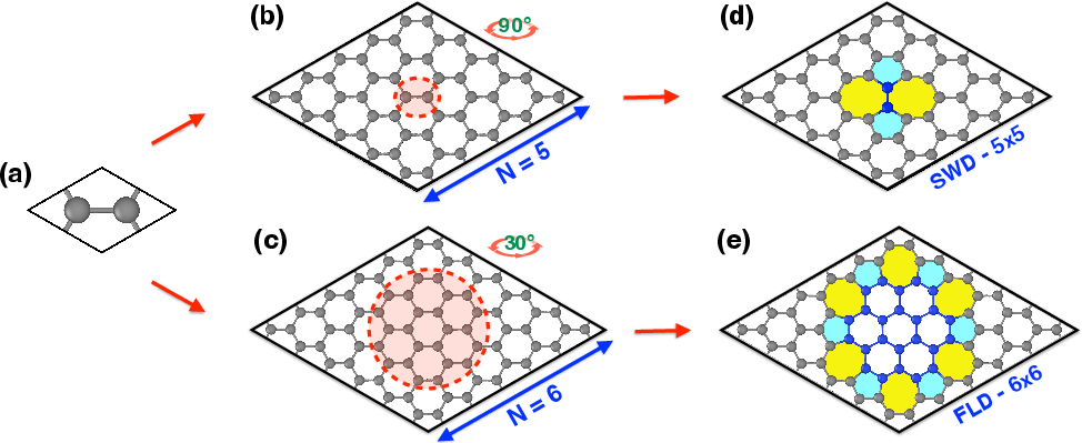
Figure 1: Workflow for constructing SWD and FLD superlattices by generating N×N supercells and applying atomic rotations to define defect regions (blue: rotated atoms; yellow: heptagons; sky blue: pentagons).
First-Principles and Tight-Binding Methods
The electronic, structural, and energetic properties of the defective superlattices are computed ab initio using the r2SCAN meta-GGA functional as implemented in VASP, with further benchmarking via the HSE06 hybrid functional. For larger systems, DFTB+ is employed to extend the accessible supercell parameter space. Tight-binding models incorporating nearest-neighbor hoppings with local perturbations near the defect cores are constructed to rationalize and predict the gap-opening patterns observed in the electronic structure calculations. Structural relaxation and symmetry determination leverage robust convergence protocols to ensure accurate space group assignment post-defect introduction.
Symmetry Analysis and Band-Gap Opening Criteria
A central contribution is the rigorous derivation and validation of a symmetry-based rule for band-gap opening. The study demonstrates both analytically and by explicit calculation that the emergence of a band-gap is governed by superlattice periodicity: only when the supercell size N is a multiple of three (3N×3N superlattices) do the K and K′ Dirac points fold to the same k-point in the reduced Brillouin zone, enabling inter-valley coupling and band-gap opening. This phenomenon is independent of inversion symmetry breaking, as both SWD and FLD preserve C2 (inversion) symmetry, but is instead rooted in the way translation symmetry is reduced by the superlattice.
Cohesive Energetics and Lattice Stability
The calculations reveal that the energetic cost per atom associated with defect introduction decreases as the supercell size increases, with cohesive energies approaching those of pristine graphene in the dilute-defect limit. For comparable supercell sizes, SWD superlattices display slightly higher cohesive energies relative to FLD, despite their smaller defect atomic fraction, reflecting differential defect core stabilization.
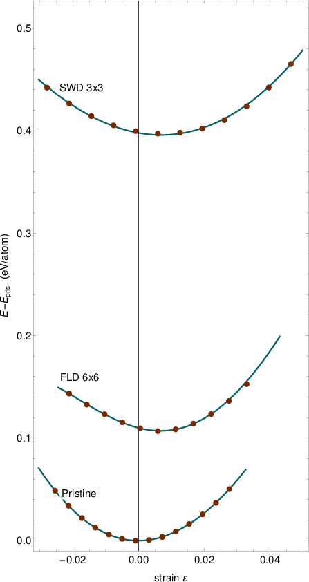
Figure 2: Total energy per atom as a function of in-plane strain for pristine graphene and selected SWD and FLD superlattices, illustrating mechanical response and defect energetics.
Electronic Structure Characterization
Stone-Wales Defect Superlattices
Electronic structure calculations for SWD lattices establish that only the N×N0 and N×N1 supercells exhibit a finite band-gap, in line with the N×N2 selection rule. The N×N3 structure displays a significant gap (N×N4 eV with rN×N5SCAN, N×N6 eV with HSE06), whereas for N×N7 the gap nearly closes as defect density decreases. Other periodicities—despite local suppression of the DOS near the Fermi level—are strictly gapless, as confirmed by fine N×N8-space analyses.
Flower-Like Defect Superlattices
FLD superlattices demonstrate more pronounced and tunable band-gaps relative to SWD, with gaps of N×N9 eV (N×N0SCAN) and N×N1 eV (HSE06) for N×N2 periodicity, and N×N3 eV for N×N4. DFTB+ calculations extend this trend to larger periodicities, confirming the selection rule and the systematic reduction of N×N5 with increasing N×N6. In all cases, the band-gap closes as the system asymptotically approaches pristine graphene for large N×N7. Notably, the gap is always direct and located at the Brillouin zone center (N×N8) for the gapped superlattices.

Figure 3: (a) Band structure of FLD--N×N9 superlattice revealing a direct band gap at 20; (b) Real-space visualization of 21 states highlighting defect core localization.
Real-Space Electronic Structure and Experimental Signatures
The defect-localized electronic density near the Fermi level is visualized, showing strong concentration on atoms forming the defect core, particularly the 22 orbitals. Simulated STM maps at varied bias voltages confirm that these localized states dominate tunneling contrast above the defect regions, providing a route to experimental detection of such defect-induced modifications.
Structural Symmetry and Gap-Opening Mechanism
Both SWD and FLD lattices retain 23 symmetry in the relaxed geometry, which precludes gap-opening via inversion symmetry breaking. Instead, the mechanism depends strictly on translation symmetry reduction; only when superlattice periodicity enforces Brillouin zone folding such that 24 and 25 coincide does inter-valley coupling—and thus gap opening—occur. For supercells not satisfying the 26 rule, Dirac cones remain isolated and massless by symmetry, regardless of defect density.
Implications and Outlook
The strong dependence of band-gap formation on supercell symmetry, rather than defect type or sublattice asymmetry, fundamentally reframes the paradigm of band-gap engineering in graphene. These findings provide an explicit design principle for constructing gapped graphene via topological defect patterning: only select superlattice periodicities can enable finite and controllable 27, with energetic and mechanical robustness confirmed by first-principles calculations. Experimentally, controlled synthesis of such periodic defect arrays (e.g., via templated growth or irradiation) would enable integration of graphene into semiconducting device platforms while preserving in-plane 28-bonding coherence. Moreover, the methodologies and symmetry analysis presented are immediately extensible to broader classes of 2D Dirac materials, including engineered superlattices in TMDCs and hBN, or the design of Kekulé-distorted phases.
Conclusion
This work establishes a predictive symmetry-based framework for gap engineering in graphene via periodic topological defects. Superlattice periodicity determines the coupling of Dirac cones and thus band-gap formation, with only 29 periodicity permitting a finite gap through Brillouin zone folding and valley hybridization. Both SWD and FLD superlattices obey this symmetry selection rule, and the resulting gaps—up to N0 eV for FLD structures—are robustly characterized via ab initio and tight-binding calculations. This symmetry-guided approach simultaneously clarifies underlying mechanisms and delineates concrete pathways for scalable, tunable semiconducting graphene, with direct translation to other designer 2D electronic materials.