- The paper demonstrates that growth-induced Se vacancies critically impact ferroelectric switching in CVD-grown 3R-WSe₂ bilayers.
- It employs graphene FE-FET structures to quantitatively track polarization switching via hysteresis and quantum Hall measurements.
- Domain dynamics and trap kinetics modulate the FE response, providing insights for scalable non-volatile memory device design.
Impact of Disorder and Multi-Domain Kinetics on Sliding Ferroelectricity in CVD-Grown 3R-WSe₂ Bilayers
Introduction and Motivation
The exploration of sliding ferroelectricity in layered van der Waals (vdW) materials is advancing the engineering of ultra-scaled non-volatile memory devices. Bilayer transition metal dichalcogenides (TMDs), and in particular the 3R-stacked polymorph of WSe₂ grown by chemical vapor deposition (CVD), offer the potential for scalable integration of out-of-plane ferroelectric (FE) behavior via the breaking of inversion symmetry through controlled stacking. While the fundamental physics of sliding FE in exfoliated 2D crystals has been reported, large-scale synthesis using CVD introduces a nontrivial landscape of structural disorder and domain configurations that directly impact the functional characteristics and ultimate device reliability of FE-based applications.
This work systematically probes the FE switching properties of CVD-grown 3R-WSe₂ bilayers, employing a graphene Ferroelectric Field-Effect Transistor (FE-FET) structure where the polarization-induced charge in the TMD modulates the resistance of an adjacent graphene channel. The investigation addresses how intrinsic disorder from growth-induced defects and multi-domain kinetics modify the FE response, thereby revealing critical factors for device design and optimization at the wafer scale.
Experimental Architecture
CVD-grown bilayer WSe₂ films with 3R stacking were integrated into heterostructures composed of graphene/hBN/3R-WSe₂ on SiO₂/Si substrates. The hBN layer serves as a critical spacer mitigating interfacial charge inhomogeneity and scattering at the graphene channel, thus enabling high-fidelity electrostatic sensing of TMD polarization switching. Device fabrication and characterization—leveraging Hall bar configurations and low-temperature cryogenic transfer measurements—permit extraction of the detailed charge transport response to out-of-plane polarization changes.
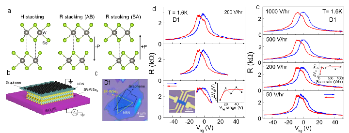
Figure 1: (a) Atomic arrangements in hexagonal and rhombohedral WSe₂ bilayers; only the 3R (rhombohedral) stacking yields out-of-plane polarization due to broken inversion symmetry. (b) Schematic of the device stack and (c) optical micrograph of a fabricated heterostructure. (d-e) Gate-dependent resistance measurements reveal clear hysteretic shifts in the graphene channel, tracking FE switching.
Polarization Switching, Disorder, and Trap Dynamics
Charge transport in graphene as a function of gate voltage exhibits pronounced hysteresis at cryogenic temperatures (T=1.6K), a direct signature of FE switching in the underlying 3R-WSe₂ (Fig. 1). The extracted 2D polarization values, on the order of 2.61×10⁻¹²C/m, quantitatively affirm substantial out-of-plane dipole formation. This hysteresis persists as gate voltage sweep range and scan rate are varied across a broad window, indicative of robust FE retention against single-domain switching kinetics.
Landau fan analysis under magnetic fields confirms that the FE-induced charge modulation in graphene shifts the Fermi level and controls Landau level (LL) filling, with the quantum Hall effect inheriting the hysteretic memory of the underlying FE (Figure 2). Notably, LL broadening and mixing of longitudinal and Hall conductances in the electron-doped regime highlight substantial disorder, primarily attributed to selenium vacancy defects in CVD-grown WSe₂. These vacancies introduce localized charge trap states near the valence band maximum, manifesting as a fluctuating interfacial charge layer (ICL) that screens both the gate and polarization fields.
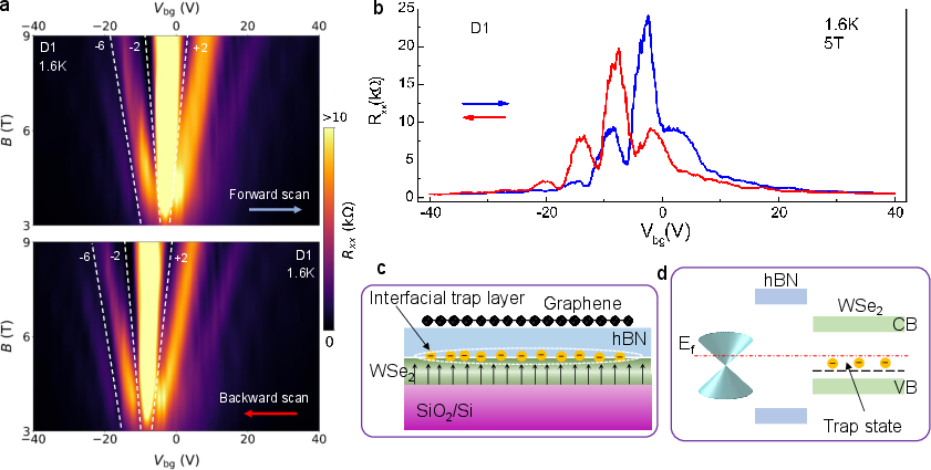
Figure 2: (a) Landau fan diagrams for graphene showing polarization-dependent quantum Hall minima. (b) Rxx traces reveal sweep-direction-dependent LL shifts. (c-d) Schematic depiction of defect-mediated ICL formation and resultant band alignment.
Temperature-dependent R-Vbg curves (Figure 3) capture a transition from conventional hysteresis at low T to anti-hysteresis at elevated temperatures (T≳80K). This transition is not intrinsic to FE switching but arises from the thermally activated trapping/detrapping kinetics of the Se vacancy-induced ICL, which at high T becomes sufficiently rapid to counteract or even overcompensate the FE-induced field, thus inverting the hysteresis loop in graphene transport. Analytical modeling of the net carrier density as a combined function of gate voltage, FE polarization, and dynamically varying trap population captures these trends.
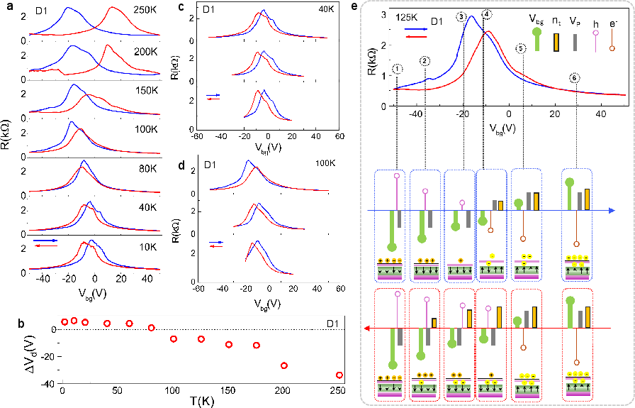
Figure 3: (a) Temperature-driven switch from hysteresis to anti-hysteresis in device transfer curves, (b) quantification of Dirac point shift △Vd, and (e) conceptual field-balance diagrams revealing the interplay of gate, polarization, and trap contributions.
Multi-Domain Switching Kinetics
Beyond the single-domain regime, multi-domain FE WSe₂ samples manifest distinct gate sweep dependence and resistance jumps at low sweep rates and low temperature, indicating relaxation and partial back-switching of FE domains (Figure 4). In these devices, at slow gate sweeps, domain dynamics rather than trap states dominate the anti-hysteretic response, characterized by abrupt resistance jumps linked to domain wall motion and relaxation events. At faster sweep rates or elevated temperatures, domain immobilization yields a conventional hysteresis, underscoring the crossover from extrinsic (domain-driven) to intrinsic (trap-driven) anti-hysteresis mechanisms.
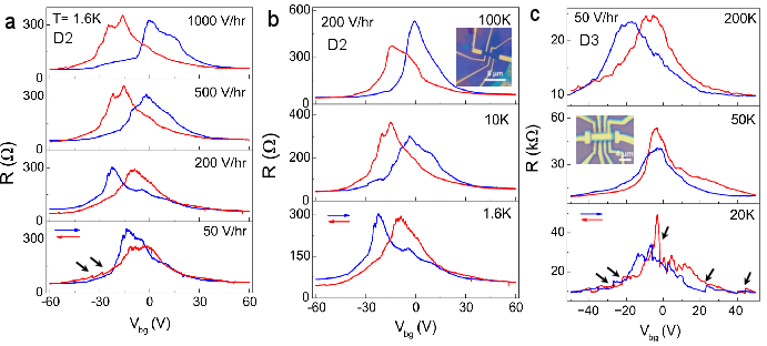
Figure 4: (a) Demonstration of sweep-rate-dependent hysteresis and resistance jumps, signifying multi-domain relaxation. (b-c) Evolution of transfer curves in multiple devices, distinguishing the interplay of domain dynamics and disorder/trap populations.
The presence of high trap densities in certain CVD-grown films obscures domain effects, as evidenced by persistent anti-hysteresis even at high temperatures, whereas devices with lower trap densities restore intrinsic domain-switching behavior.
Implications and Outlook
This study systematically establishes that intrinsic disorder—in particular, growth-induced selenium vacancies—and resulting defect-driven trap dynamics are the critical bottleneck for robust non-volatile FE switching in CVD-grown 3R-WSe₂. Multi-domain kinetics, while offering additional degrees of freedom for tunability, further modulate the switching characteristics and must be managed for deterministic device performance.
The demonstrated ability of graphene to sensitively transduce FE polarization switching, coupled with direct quantum Hall measurements, provides a comprehensive probe of both polarization state and disorder landscape. The observed order-of-magnitude shift in polarization densities, the persistence of hysteresis/anti-hysteresis over varied temperature, and the interplay of extrinsic and intrinsic screening mechanisms are salient for the practical realization of wafer-scale 2D FE memory and logic architectures.
Continued progress will require process refinements to minimize defect densities, along with the deterministic engineering of domain structures via CVD growth parameters, strain, or substrate functionalization. The nuanced anti-hysteresis phenomena also point to opportunities for device functionalities such as non-volatile charge trapping or neuromorphic behavior, contingent on the controllability of trap populations and domain kinetics.
Conclusion
The comprehensive transport and quantum Hall investigation of CVD-grown 3R-WSe₂ bilayers reveals that disorder dynamics—dominated by Se vacancies—and multi-domain FE kinetics fundamentally determine the polarization switching characteristics in 2D vdW ferroelectrics. These findings delineate the operational limits and optimization pathways for scalable FE-based memory and logic devices, cementing the importance of both materials growth control and electronic probe design for next-generation nanoelectronic platforms.
Reference:
"Impact of Disorder Dynamics and Multi-Domain Kinetics on the Sliding Ferroelectricity of CVD-Grown 3R-WSe₂ Bilayers" (2606.00665)