- The paper presents a detailed atomistic study using a new DFT-trained ReaxFF force field to quantify electric field effects on defect migration in GaN.
- It reveals that linear dipole approximations fail as electric fields induce nonlinear, anisotropic responses in vacancies and interstitials.
- Results show that even small barrier reductions significantly enhance defect mobility, impacting GaN device reliability under high operating fields.
Electric-Field Effects on Defect Migration Energetics in GaN
Introduction
This work delivers a comprehensive atomistic investigation of electric field effects on point defect migration in gallium nitride (GaN) via large-scale reactive molecular dynamics (MD) leveraging a new ReaxFF force field, parameterized from an extensive DFT dataset. The context is set by the urgent need to understand defect kinetics under high-field and radiation exposure, critical for the reliability of GaN-based power and RF electronics. A major focus is the dynamical coupling between local charge, lattice distortion, and defect migration energetics, especially under high external electric fields (up to the dielectric breakdown limit). The paper asserts that prevailing linear dipole-field approximations are insufficient, with nonlinear, anisotropic responses observed for various intrinsic defects.
ReaxFF Force Field Development and Validation
A new ReaxFF parameterization for GaN was generated using DFT-trained reference data, encompassing various Ga and GaN polymorphs and molecular nitrogen, as well as a wide suite of defect configurations (vacancies, interstitials, antisites, Frenkel pairs, Schottky defects). Equation-of-state (EOS) curves from ReaxFF closely track DFT for both wurtzite GaN and reference phases. For wurtzite GaN, the predicted lattice constants and bulk modulus agree with DFT and reported experiment within a few percent.
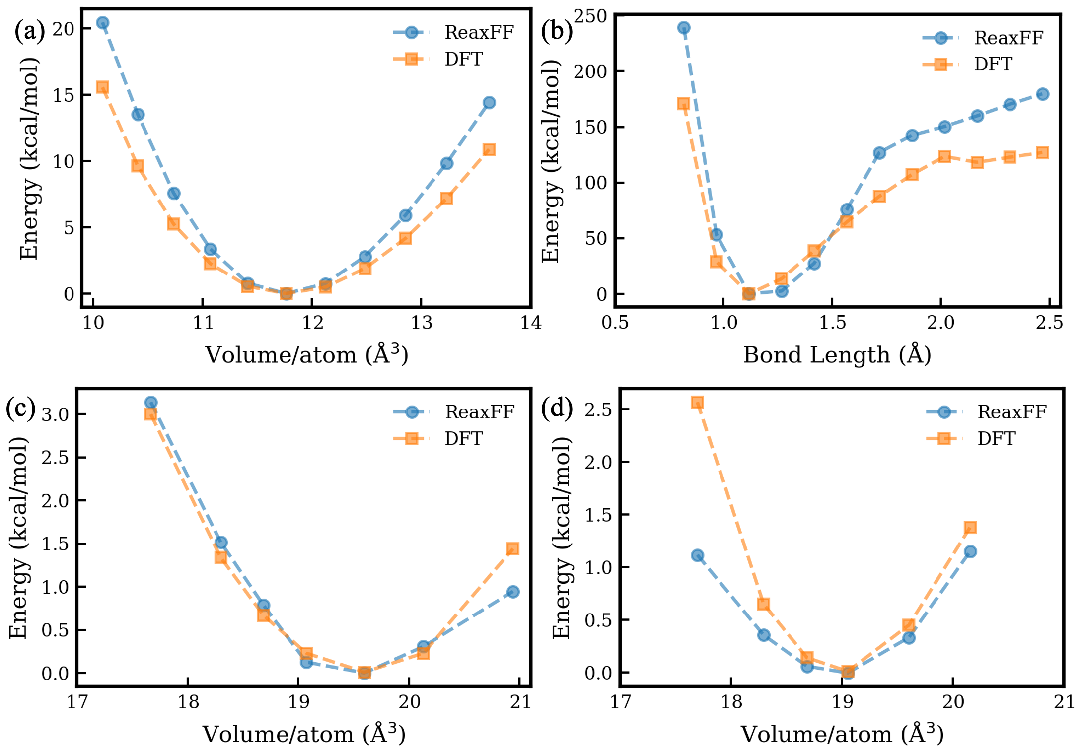
Figure 1: EOS data for wurtzite GaN and validation against DFT reference.
Defect formation energies, an important reliability benchmark, show generally strong correspondence to DFT, with deviations under 26% across defect classes—with maximum discrepancies for vacancy types.
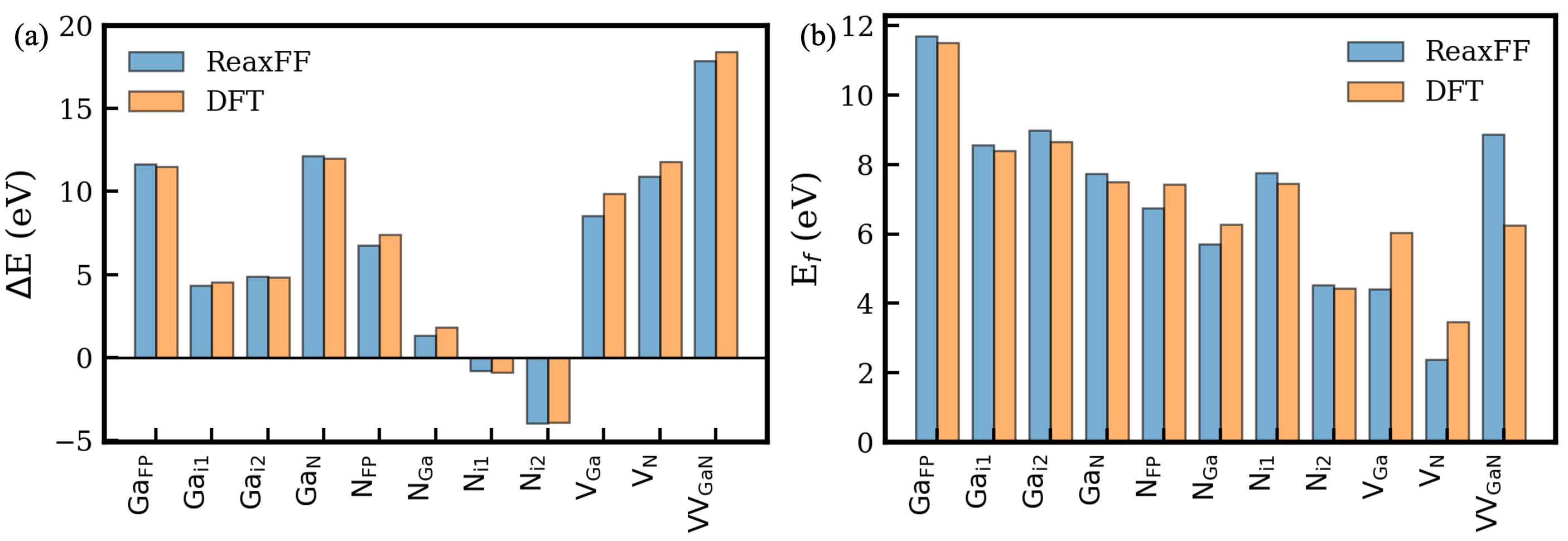
Figure 2: (a) Comparison of total energies for defective vs. pristine supercells; (b) Defect formation energies under N-rich conditions for both ReaxFF and DFT.
Benchmarking Defect Migration Barriers
The study calculates migration barriers for the most relevant native point defects using climbing-image NEB under the newly parameterized potential. Both in-plane and out-of-plane migration paths are considered, with a focus on the dominant pathways for vacancies and interstitials, corroborated by multiple prior first-principles works.
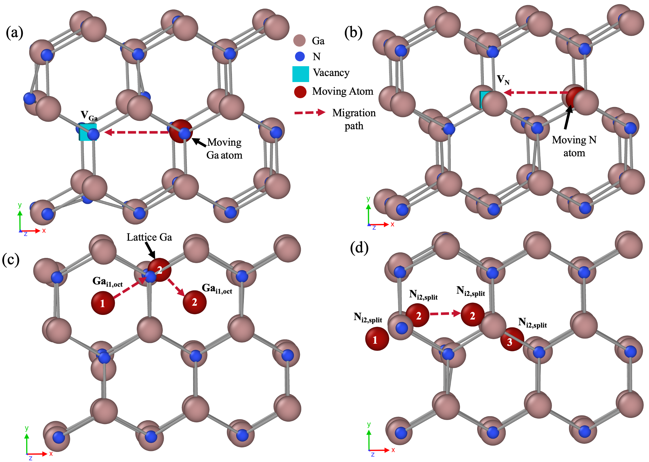
Figure 3: Schematics of migration directions for (a) Ga vacancy, (b) N vacancy, (c) Ga interstitial, and (d) split nitrogen interstitial.
Calculated zero-field migration barriers for neutral defects align with published DFT and experimental data: VGa at 2.35 eV, VN at 2.17 eV, Gai1,oct at 0.88 eV, and Ni2,split at 1.03 eV.
Electric Field Effects on Migration Energetics
A core contribution is the systematic characterization of how externally applied electric fields modulate migration barriers for each defect, up to fields of 0.04 V/Å (40 MV/cm, exceeding typical device breakdown).
Vacancies
For VGa, the field parallel to the migration path increases (forward) and decreases (reverse) the barrier, but slope asymmetry (0.15 eV vs. 0.10 eV) signals a breakdown of the rigid dipole-field assumption. Analysis reveals that significant field-induced local charge redistributions and lattice strains, sustained through migration, produce these nonlinearities.
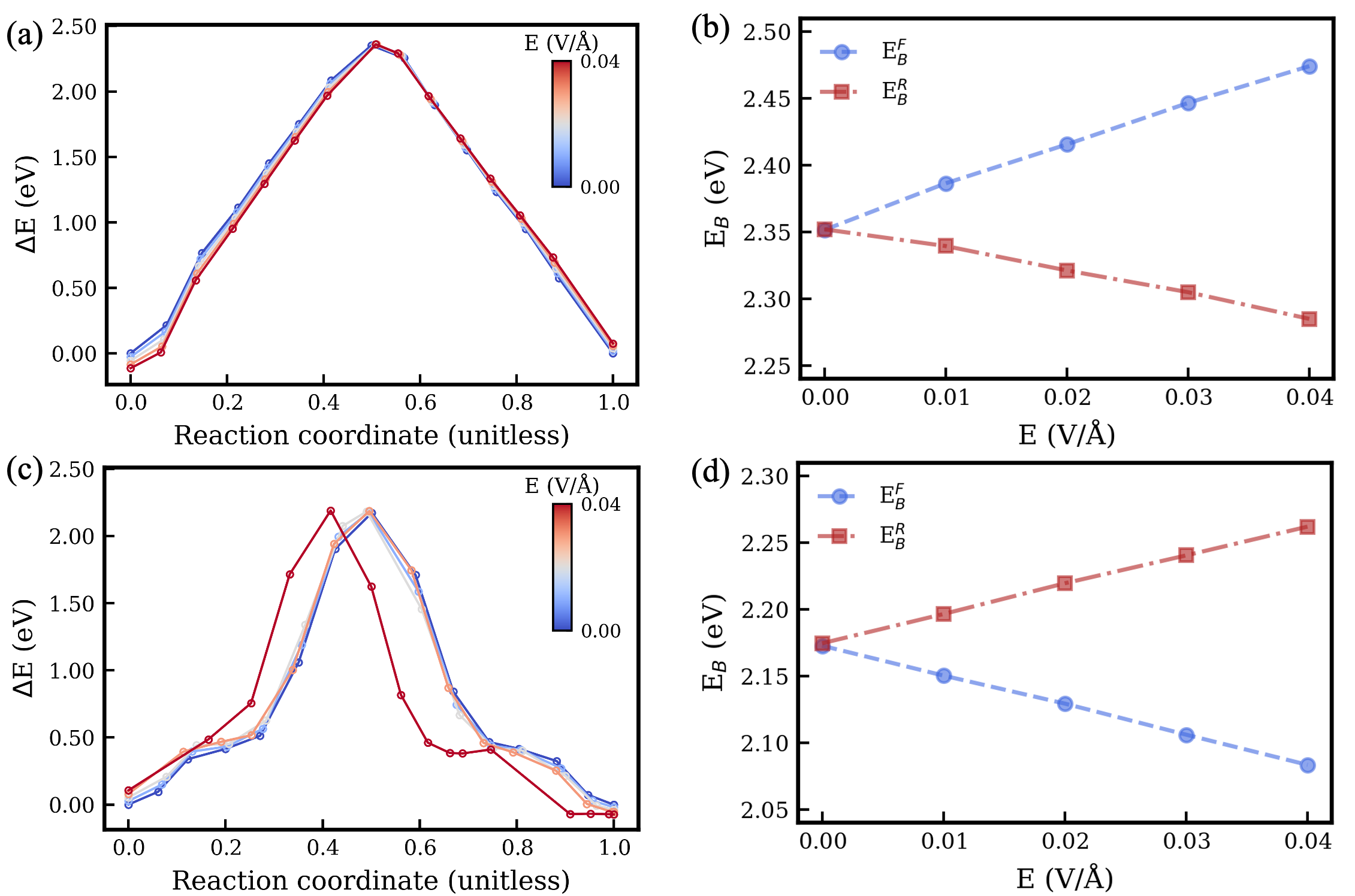
Figure 4: Electric field dependence of migration barrier and energy landscape for VGa with field along the x-direction.
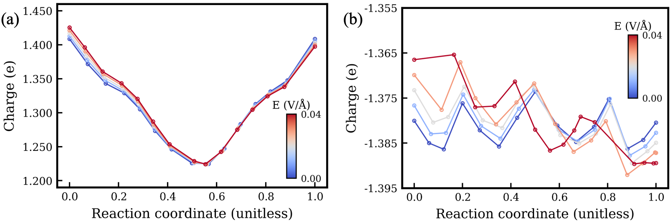
Figure 5: Charge state evolution for the migrating atom in Ga vacancy under increasing electric field.
For VN, the response is almost perfectly linear and symmetric, matching theoretical expectations for a point defect with minimal lattice coupling.
Interstitials
The Ga interstitial (Gai1,oct) demonstrates a qualitatively different energy landscape under field: the number and position of saddle points (rate-limiting) shift as the field increases, with pronounced, highly nonlinear modulation of both forward and reverse barriers. Notably, the reverse barrier is affected more strongly, and both the migration trajectory and coupled multi-atom charge redistribution drive these deviations.
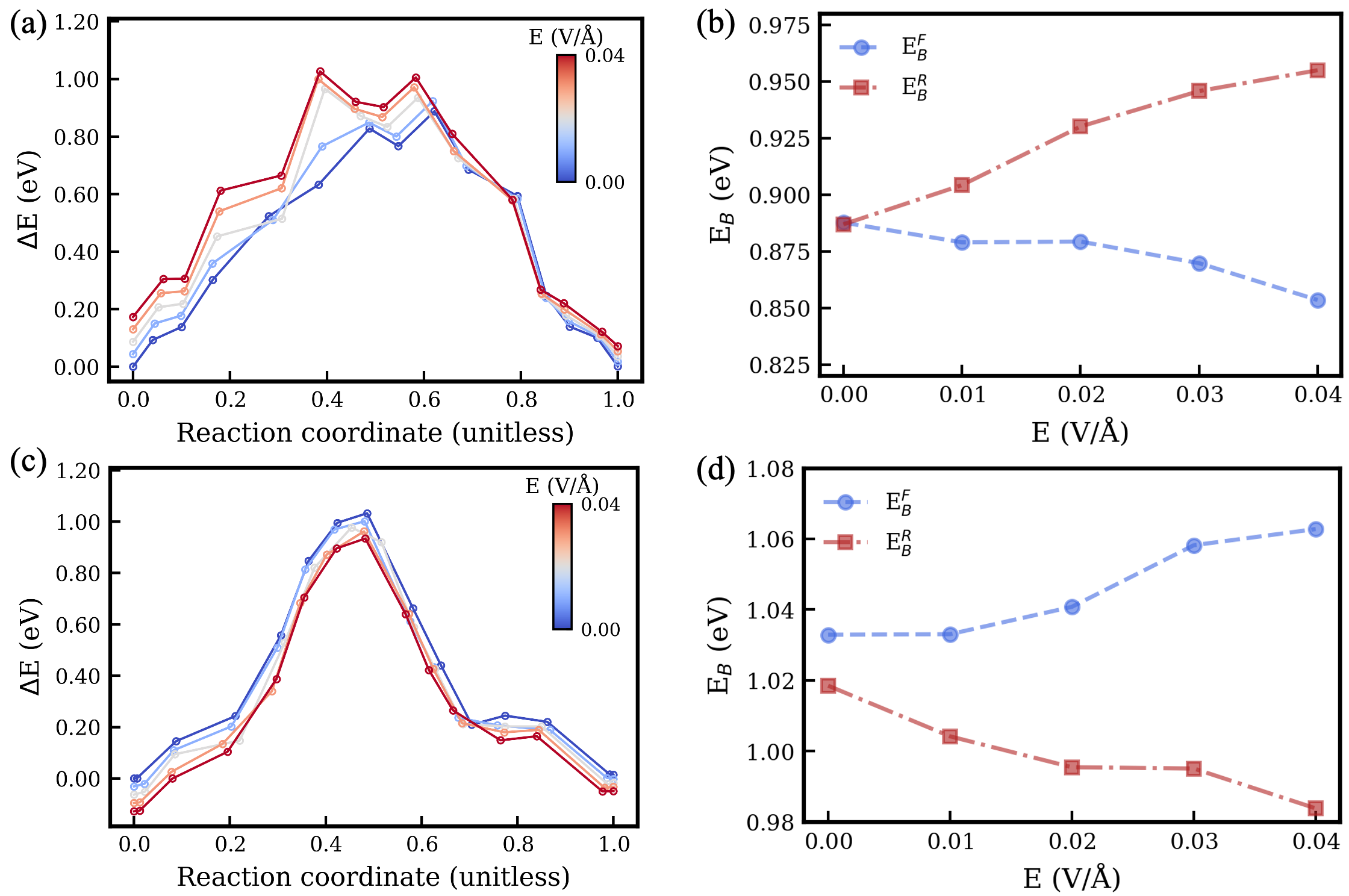
Figure 6: Electric field effects on migration barrier profile for Gai1,oct interstitials.
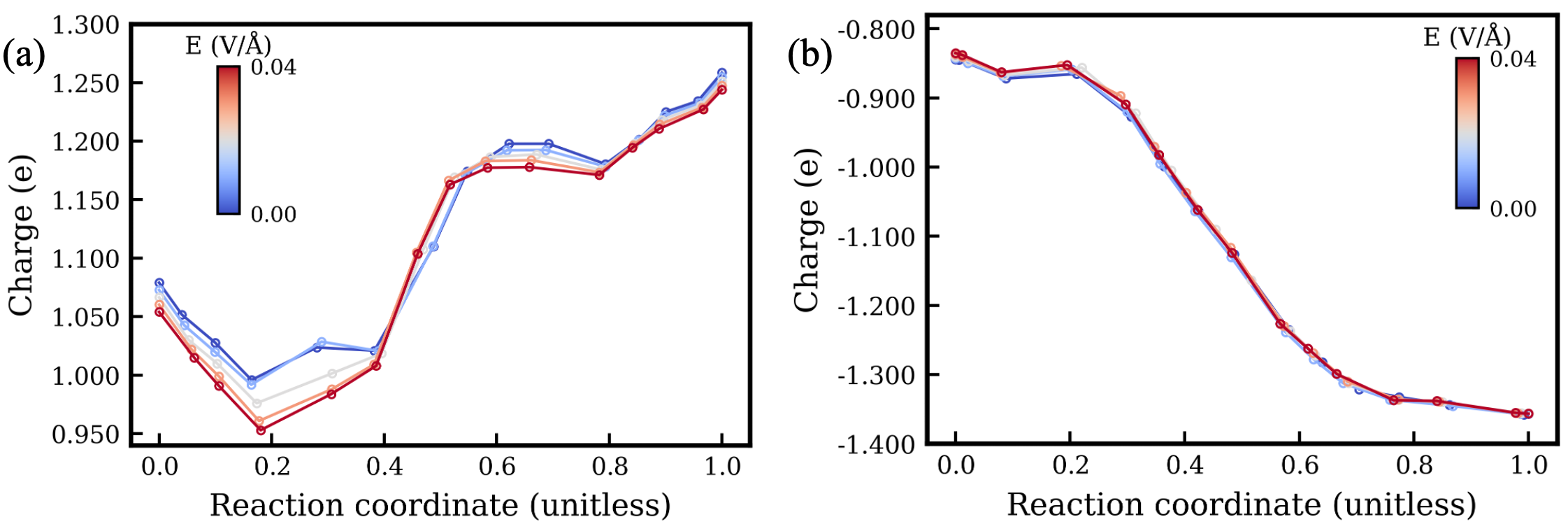
Figure 7: Electric field-driven charge state dynamics for the moving atom in Ga interstitial migration.
Split nitrogen interstitials behave similarly, with strong nonlinearity, asymmetry, and significant deviations from the linear dipole response—particularly notable for migration directions canted with respect to field orientation.
Theoretical Implications
The findings compellingly demonstrate that a linear dipole-field coupling—or any constant effective dipole approach—is inadequate for modeling defect migration in polar/ionic semiconductors like GaN. The effective dipole moment, partial charges, and lattice strain all evolve continuously along the migration path and exhibit strong sensitivity to both defect type and electric field directionality. These effects are attribute-specific:
- Vacancies (VN0, VN1): Responses range from nearly symmetric and linear (N) to mildly asymmetric (Ga), depending on the depth and degree of lattice distortion and charge variation.
- Interstitials: Nonlinear response is driven by multi-atom cooperative effects and complex field-mediated charge/lattice coupling.
The kinetic consequences are significant: field-induced reductions of even 0.05 eV in the barrier (as observed for interstitials) can alter diffusion rates by an order of magnitude at device operating temperatures, directly impacting reliability, especially under the persistent high fields of HEMTs and vertical GaN devices.
Practical Ramifications for GaN Technology
These results have immediate consequence for the long-term reliability and performance limitations of GaN-based power and radiation-hardened electronics. Specifically:
- Enhanced Defect Mobility: Interstitials with room-temperature migration thresholds (N21 eV) become highly mobile under operational fields, likely contributing to dynamic degradation pathways such as trap generation, threshold voltage shift, and gate leakage.
- Directional Defect Drift: Net migration asymmetries suggest electric-field-driven accumulation of defects at critical device regions such as interfaces or gate edges, accelerating failure processes.
- Radiation/High-Power Context: For environments with substantial displacement damage or where charge-state control is limited, these effects are expected to be even more pronounced, possibly activating new failure or compensation mechanisms.
The study thus motivates new models in device reliability analysis that account for nonlinear, defect- and field-specific migration kinetics.
Methodological Considerations and Outlook
While ReaxFF with QEq charge equilibration provides access to large system sizes/unprecedented spatial statistics, limitations include the absence of explicit charge-state quantization (as in DFT) and the inability to resolve charge-state transitions under high field. As a result, these findings represent a lower bound on field response, and the migration of highly charged defects—in practice, dominant for n-type GaN under bias—may exhibit even more substantial nonlinearities. Extension to ML-based interatomic potentials with explicit charge state handling represents a promising avenue for future research.
Conclusion
Through the development of a DFT-trained ReaxFF force field and systematic study of field-driven defect migration, this work demonstrates that electric fields do not induce a simple linear bias on migration barriers in GaN. Rather, they induce complex, anisotropic, and nonlinear responses, with strong defect-specificity, arising from local charge redistribution and lattice effects. For interstitials, these dynamics are sufficient to substantially alter diffusion-driven degradation kinetics, with direct relevance to the design and reliability of future GaN-based devices under realistic operational and irradiation conditions.