- The paper demonstrates that nanoscale strain in MoS₂/Au(111) massively enhances light-induced bandstructure renormalization and quantum particle localization.
- It employs STM/STS measurements alongside tight-binding and molecular dynamics simulations to quantify local LDOS enhancements and a bandgap reduction exceeding 150 meV.
- The findings establish design principles for harnessing plasmon-enhanced photodoping to engineer nanoscale quantum emitters and solid-state quantum simulators.
Strongly Enhanced Electronic Bandstructure Renormalization by Light in Nanoscale Strained Regions of Monolayer MoS₂/Au(111) Heterostructures
Introduction
This work systematically investigates quasiparticle (QP)-mediated bandstructure renormalization in monolayer (ML) MoS₂ on Au(111) heterostructures, with a particular focus on regions of the MoS₂ monolayer subjected to nanoscale strain by underlying substrate corrugations. Using combined scanning tunneling microscopy/spectroscopy (STM/STS) under optical illumination, the study elucidates the dynamic interplay between photoexcited carrier localization, strain-induced bandstructure modulation, and energy-funneling in the strained monolayer. A theoretical framework based on tight-binding Hamiltonians, extracted from first principles and parametrized by molecular dynamics-derived strain fields, is developed to quantitatively describe these phenomena.
The enhanced many-body interactions characterizing TMDs in the 2D limit can fundamentally alter QP binding and interaction strengths. While this has been widely studied in unstrained or micron-scale modulated systems, this study demonstrates that nanoscale strain leads to far deeper energy modulation, facilitating strong spatial localization and accumulation of photoexcited QPs, and strongly amplifying local opto-electronic functionality.
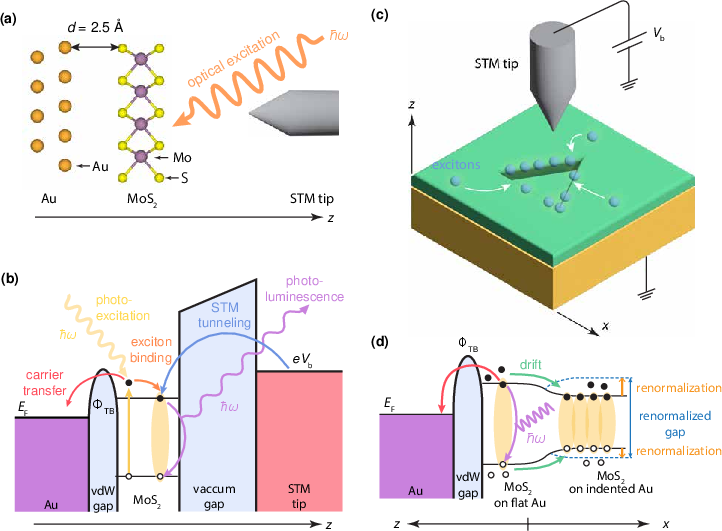
Figure 1: Schematic of STM/STS setup for optically excited MoS₂/Au(111), associated energy diagrams, and illustrations of QP aggregation and carrier pathways determined by nanoscale strain fields.
Morphological and Electronic Structure Characterization
The Au(111) substrate introduces significant surface corrugations, resulting in MoS₂ flakes that are both microns in extent and have pronounced nanoscale height fluctuations. These yield both Moiré superlattice patterns and discrete, atomically sharp step edges and corner-like nanoscale indentations (Figure 2). STM/STS demonstrates that the electronic bandgap in unstrained, flat regions of the heterostructure is 1.8–1.82 eV, and that the ML-MoS₂ exhibits n-type doping due to Fermi level pinning near the conduction band.
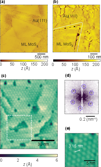
Figure 2: Topography and Moiré patterns of ML-MoS₂/Au(111), highlighting strained morphologies and nanoscale wrinkles induced by substrate heterogeneity.
Experimental differential conductance spectra confirm the theoretically predicted band structure (Figure 3), and distinctive spectral features associated with the K- and Q-valleys are observed.
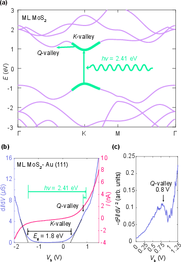
Figure 3: Calculated ML-MoS₂ band structure and representative dI/dV tunneling spectra. The Q-valley feature appears as an LDOS kink 0.8 eV above EF.
Strain-Induced Structural and Electronic Modulation
The nanoscale sharp features in Au(111) (e.g., single- and double-layer step indentations) impart localized, high-gradient strain fields in overlying MoS₂, as directly visualized by STM and modeled by MD simulation (Figure 4). Notably, the out-of-plane strain tensor component uzz is maximized at atomically sharp edges and corners, where the bandgap modulations are largest and the LDOS is strongly enhanced. Sharper (i.e., smaller angle) corners amplify the uzz strain and the corresponding LDOS enhancement.
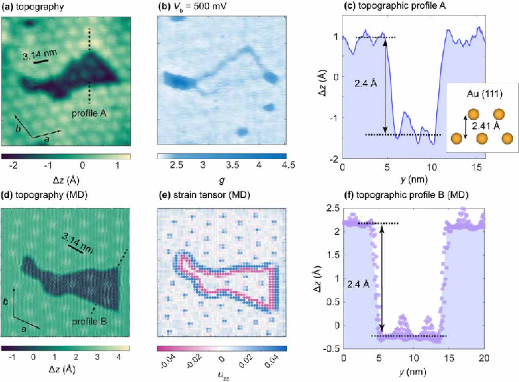
Figure 4: Correlation of Au(111) topographic step features, MD-simulated MoS₂ conformation, and calculated strain fields—most strongly pronounced at step edges/corners.
Such strain localization drives local flattening of the conduction and valence bands, shrinking the gap and funneling QPs into these lower-energy wells. STM maps reveal a pronounced spatial variation in the LDOS that correlates precisely with strain-gradient features.
Light-Induced Electronic Renormalization: Spatial Control by Nanoscale Strain
Under illumination (515 nm laser), normalization of the tunneling conductance reveals substantial light-induced LDOS enhancements that are highly localized to the strained nanoscale features (Figures 5, 6). This renormalization is negligible in unstrained or weakly strained regions but can be several times larger within ~5–10 nm of a high-strain edge/corner.
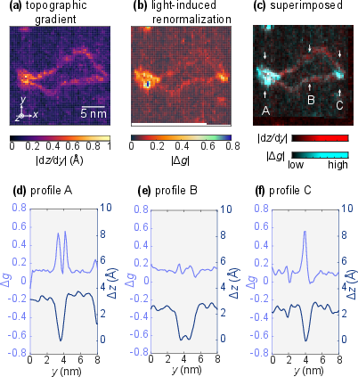
Figure 5: Spatial correlation of gradient topography and light-induced LDOS renormalization. Profiles confirm maximal enhancement at strained edge features.
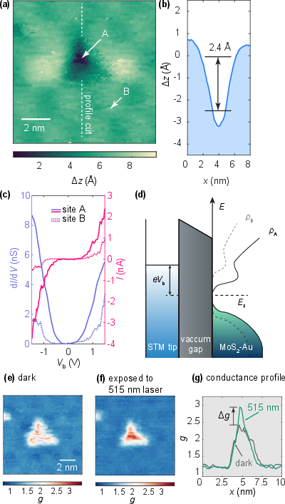
Figure 6: Single triangular indentation geometry; side-by-side comparison of LDOS and dI/dV in flat versus strained regions, and bias-dependent conductance maps under dark/illuminated conditions.
The observed LDOS renormalization is attributed to the enhanced local QP density—exciton, trion, and electron-hole plasma populations—in strain-defined nanoscale energy wells. These QPs accumulate on timescales longer than the plasmonically-enhanced optical-pumping and exciton formation times, and shorter than the out-of-plane tunneling and radiative recombination, resulting in a pronounced, steady-state carrier population well-approximated by a local equilibrium subject to strong many-body coupling.
Quantitative Theoretical Framework and Bandstructure Engineering
The electronic structure is computed with a real-space tight-binding superlattice Hamiltonian, parametrized by first-principles-derived hopping integrals, and the strain field extracted from MD. This approach captures both the global Moiré superlattice modulation and the highly localized, inhomogeneous strain of indentations (Figure 7).
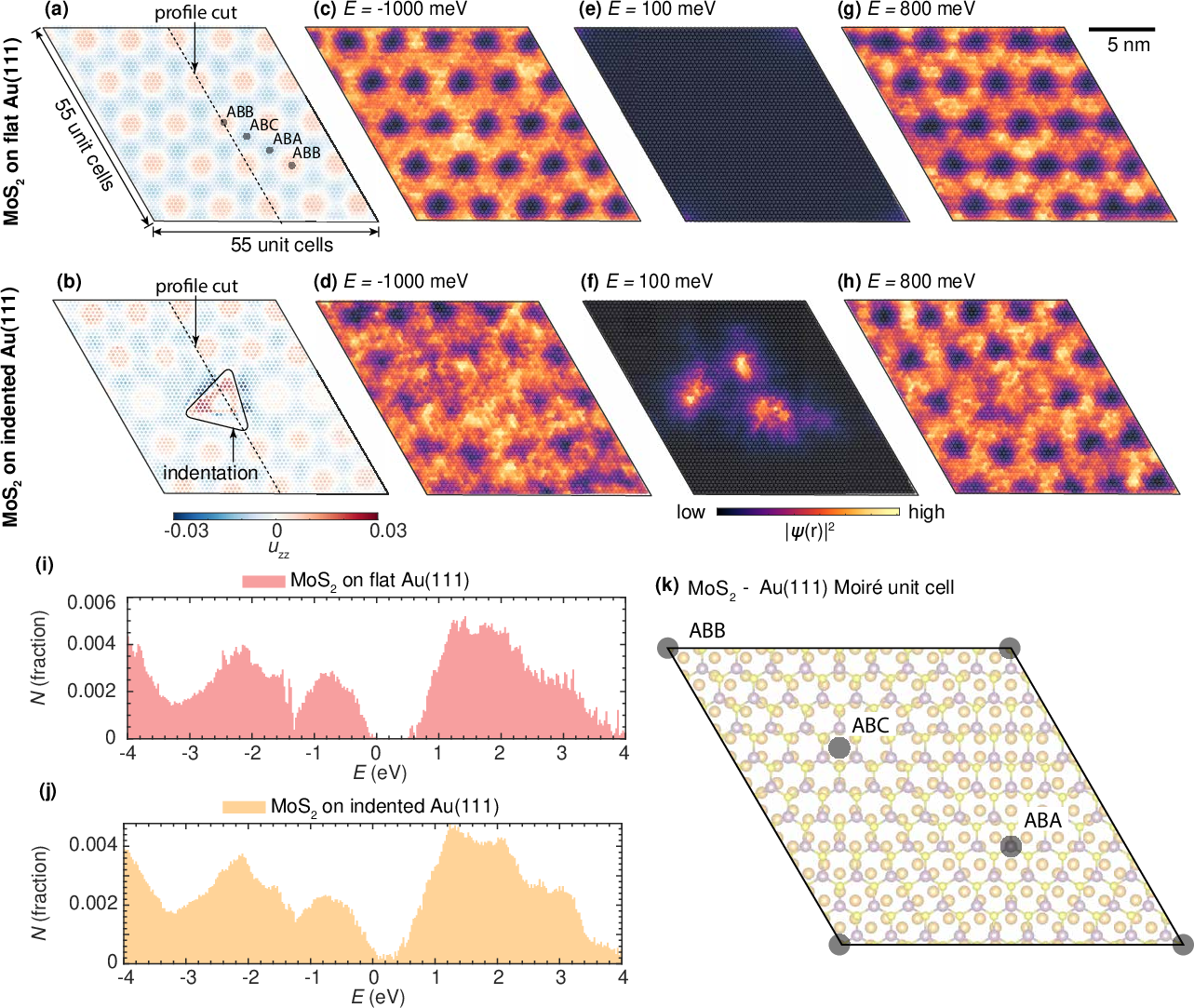
Figure 7: Calculated strain tensors and resulting electron probability densities for flat and indented regions; eigenvalue spectrum (global DOS) showing reduced gap and smearing with increasing strain inhomogeneity.
Electron probability densities at energies within the conduction/valence bands and in the gap further validate the spatial concentration of electronic states—localization is enhanced in the regions most subject to out-of-plane bending and strain.
Complementary analysis shows that the bandgap can be reduced by more than 150 meV (local Eg shrinkage) for strain on the order of ±3%, with substantial redistribution of the LDOS and the suppression of the nominal “zero-LDOS” region near EF.
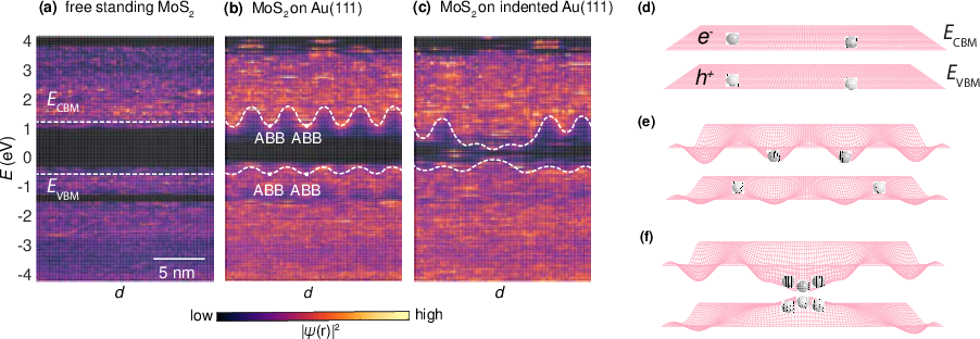
Figure 8: Calculated spatial electron distribution maps at different energies—flat, weakly modulated, and strongly strained/indented regimes; schematic energy landscapes show QP funneling mechanisms.
Bias and Laser Power Dependence, Role of Plasmonic Enhancement
Further spatially resolved tunneling experiments as a function of bias and laser power reveal that:
- The magnitude of light-induced renormalization increases systematically with both STM bias and optical power, saturating in highly strained regions (Figures 9, 10).
- Field-enhancement by tip-sample plasmon resonance in the metal/dielectric/metal junction is crucial—numerical simulations indicate optical electric fields can be enhanced by 2–3 orders of magnitude in the STM gap region, enabling strong nonlinear optical-QP coupling at sub-mW/cm² incident powers.
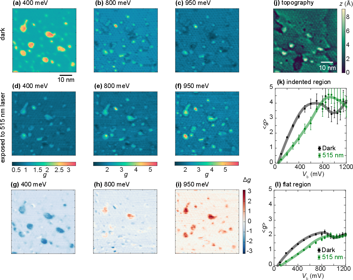
Figure 9: Bias dependence of conductance change under dark/laser illumination, mapped for both indented and flat regions, with the strain-localized enhancement persisting across a wide energy window.
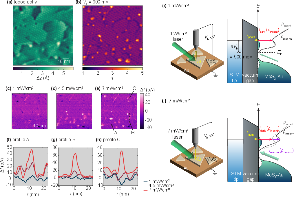
Figure 10: Laser power series for the same region, showing highly nonlinear enhancement of ΔI in strained sites compared to flat areas.
Theoretical and Practical Implications
This work demonstrates—using both experiment and multi-scale theoretical modeling—that nanoscale strain engineering in TMD/metal heterostructures enables deterministic, spatially localized enhancement of many-body optoelectronic effects. The extreme localization, well below the optical wavelength, offers a route to:
- Quantum-confined regions of high QP density for tunable quantum emitters with addressable energies and narrow spatial footprints.
- Tailored nanoscale trapping potentials for solid-state exciton-polariton quantum simulation architectures.
- Site-selective bandgap modulation and energy funneling schemes relevant for ultra-compact optoelectronic and photonic integration.
By systematically quantifying the interplay of QP dynamics, strain, and local rehybridization of the bandstructure in realistic, structurally complex ML-MoS₂/Au(111) systems, this study establishes a design principle: atomically localized strain, coupled with plasmon-enhanced photodoping, achieves maximal electronic tunability for nanoscale quantum technologies.
Conclusion
This study reveals that optically induced electronic bandstructure renormalization in monolayer MoS₂ on Au(111) is strongly and spatially localized by nanoscale strain. High-gradient out-of-plane corrugations in the substrate transform the local energy landscape, funneling QPs and amplifying photo-induced many-body effects at regions as small as a few nanometers. These findings provide a robust, experimentally accessible framework for the deterministic engineering of QP localization and energy landscape tailoring in van der Waals heterostructures, with profound implications for the development of scalable, energy-adjustable quantum optoelectronic devices, tunable quantum light sources, and solid-state quantum simulators based on 2D materials (2410.02047).