Direct Generation of an Array with 78400 Optical Tweezers Using a Single Metasurface
Abstract: Scalability remains a major challenge in building practical fault-tolerant quantum computers. Currently, the largest number of qubits achieved across leading quantum platforms ranges from hundreds to thousands. In atom arrays, scalability is primarily constrained by the capacity to generate large numbers of optical tweezers, and conventional techniques using acousto-optic deflectors or spatial light modulators struggle to produce arrays much beyond $\sim 10,000$ tweezers. Moreover, these methods require additional microscope objectives to focus the light into micrometer-sized spots, which further complicates system integration and scalability. Here, we demonstrate the experimental generation of an optical tweezer array containing $280\times 280$ spots using a metasurface, nearly an order of magnitude more than most existing systems. The metasurface leverages a large number of subwavelength phase-control pixels to engineer the wavefront of the incident light, enabling both large-scale tweezer generation and direct focusing into micron-scale spots without the need for a microscope. This result shifts the scalability bottleneck for atom arrays from the tweezer generation hardware to the available laser power. Furthermore, the array shows excellent intensity uniformity exceeding $90\%$, making it suitable for homogeneous single-atom loading and paving the way for trapping arrays of more than $10,000$ atoms in the near future.
Paper Prompts
Sign up for free to create and run prompts on this paper using GPT-5.
Top Community Prompts
Explain it Like I'm 14
Overview
This paper shows a new way to create a huge grid of “optical tweezers” using a single, very thin device called a metasurface. Optical tweezers are tiny spots of focused light that can trap single atoms, like super small hands made of light. The team built a metasurface that makes 280 by 280 tweezers at once (that’s 78,400 tweezers), with very even brightness, and without needing a big microscope lens to focus the light. This helps scale up atom-based quantum computers, which need many well-controlled atoms acting as qubits.
What questions did the researchers ask?
- Can we make far more optical tweezers than current methods, and keep them small and uniform enough to trap single atoms?
- Can a single metasurface both split light into many spots and focus those spots directly into micrometer-sized tweezers, removing the need for bulky microscope lenses?
- If we can scale tweezers this much, what becomes the new limit: the hardware or the available laser power?
How did they do it?
First, two key ideas:
- Optical tweezers: Think of these as tiny, bright dots that can hold individual atoms still. Each dot needs to be small (around a micrometer across), bright, and similar in intensity to the others so atoms can be trapped evenly.
- Metasurface: Imagine a super-thin glass chip covered in a “forest” of nanoscale pillars. Each pillar slightly changes how light passes through it—like many tiny traffic cones redirecting cars. Together, they shape the light to create thousands of focused spots exactly where you want them.
Here’s their approach in simple steps:
- Designing the light pattern with a computer
- They used a recipe (the Weighted Gerchberg–Saxton algorithm) that starts with a guess and repeatedly adjusts the “phase” pattern—how the light waves are shifted—until the simulated tweezers are evenly bright and correctly placed.
- Because the metasurface is large and very detailed, they used efficient computing tricks to handle huge calculations.
- Turning the design into a real device
- They “mapped” the desired phase shifts to pillar sizes: different pillar widths bend light by different amounts.
- Then they fabricated the pillars on a glass chip using steps common in microchip manufacturing (coating, patterning with electron beams, and etching). The pillars are tall and cleanly shaped, which is important for good optical performance.
- Testing the metasurface
- They shined an 852 nm laser (infrared) onto the metasurface, which directly focused the light into the array of tweezers a few millimeters away—no big microscope lens needed.
- They measured the spacing, size, and brightness uniformity of the spots with a camera and a small objective, checking that the tweezers matched the expected shape and quality.
What did they find and why is it important?
They successfully generated a record-large array of optical tweezers with high quality. Here are key numbers and reasons they matter:
- Scale: 280 × 280 = 78,400 tweezers. This is close to an order of magnitude more than most existing systems, which struggle beyond ~10,000.
- Focusing without a microscope: The metasurface both splits and focuses the light into micrometer-sized spots, simplifying the setup and reducing losses.
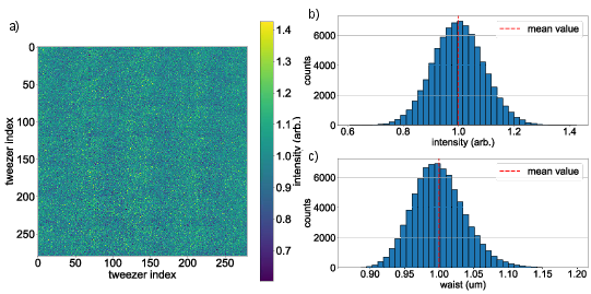
- Uniformity: Over 90% intensity uniformity across the array, which is crucial for loading many atoms consistently.
- Spot quality: Nearly diffraction-limited spots (close to the smallest physics allows), with most having high Strehl ratios (a measure of quality).
- Efficiency: About two-thirds of the light goes into the main pattern; overall light use ends up near 59%. That’s competitive or better than common alternatives.
- Spacing and size: Spots are about 4.26 µm apart, with radii around 1.0 µm—right in the range needed for trapping single atoms.
Why it matters: Atom arrays are a leading platform for building quantum computers. To get fault-tolerant quantum computers, you need many qubits (atoms) and high-quality control. Making far more tweezers that are small, even, and simpler to generate removes a major barrier. The paper shows the hardware can scale; now the main limit shifts to how much laser power you have to feed all those traps.
Implications and potential impact
- Scaling qubits: This approach can support trapping arrays with more than 10,000 atoms soon, accelerating experiments and progress in quantum computing.
- Simpler systems: Removing the large microscope objective makes setups more compact, potentially more stable, and easier to integrate.
- New bottleneck: The key challenge now is laser power. Each tweezer needs a bit of power. Even with powerful lasers today, you can reliably power tens of thousands of tweezers—but the metasurface can make even more. As lasers improve, the number of usable traps can keep growing.
- Future directions: Metasurfaces can be customized for different tasks (e.g., focusing, collecting fluorescence, or operating at multiple wavelengths), and other groups have also shown very large arrays. Together, these results suggest metasurfaces are a strong path toward truly large-scale, practical atom-based quantum machines.
Knowledge Gaps
Knowledge gaps, limitations, and open questions
Below is a single, consolidated list of what remains missing, uncertain, or unexplored in the paper. Each point is framed to be concrete and actionable for future work.
- Atom trapping not demonstrated: quantify single-atom loading probabilities, trap depths, lifetimes, temperatures, and coherence across the full 78,400-site array; validate uniform loading and site-to-site consistency.
- Rearrangement and dynamic control absent: develop and benchmark strategies for atom rearrangement and defect healing with a static metasurface (e.g., overlay AOD/SLM beams, auxiliary steerable traps, or tunable metasurfaces).
- Site-resolved addressing and readout: specify and demonstrate how to deliver tightly focused control beams and achieve single-atom imaging without a microscope objective in the proposed “lensless” architecture.
- Laser power bottleneck not mitigated: propose and test scalable power-delivery strategies (multi-laser combining, time/spectral multiplexing, beam apodization) to surpass the ≈33,000-trap limit while maintaining trap depth and uniformity.
- High-power operation untested: measure damage thresholds, thermal lensing, index drift, surface warping, and long-term reliability of silicon nitride metasurfaces at realistic intensities (≥100 W/cm²) and multi-hour operation.
- Efficiency and background light: reduce 12.9% inter-trap background and increase 58.8% total utilization efficiency; quantify impacts on atom heating and AC Stark shifts; implement and validate zero-order suppression (e.g., off-axis phase ramps, blazed designs, absorbing masks).
- Intensity uniformity gap: explain and correct the 9.4% standard deviation vs. 2.45% simulation (fabrication errors, near-neighbor coupling, undiffracted light); introduce phase pre-compensation, fabrication-aware design, and closed-loop feedback with measured wavefronts.
- NA discrepancy and trap metrics: assess how effective NA=0.51 (vs. designed 0.58) alters trap frequencies, depths, and loading; optimize incident beam size, apodization, and fill factor to reach target NA and spot size.
- Full-field aberrations and focus flatness: map axial focal position, field curvature, astigmatism, and coma across the entire ~1.19 mm array; report edge performance and quantify site-to-site optical aberrations.
- Outside-vacuum deployment feasibility: rigorously model and experimentally validate performance through realistic vacuum windows (thickness, refractive index, coatings), including spherical aberration, reflections, and back-focal distance constraints at NA≈0.5.
- Multi-wavelength functionality: design and characterize achromatic or multiplexed metasurfaces for 852 nm trapping, 780 nm fluorescence collection, and 480 nm Rydberg excitation; quantify chromatic aberration and focal shifts per wavelength.
- Polarization dependence: measure polarization-induced phase/transmittance variations and cross-polarization conversion; assess impacts on Raman transitions, state-dependent trapping, and gate fidelities.
- Electromagnetic modeling limitations: replace scalar propagation with hybrid/full-wave models that incorporate vectorial effects, substrate thickness, and meta-atom coupling; verify predictions against measured uniformity and spot quality.
- Unit-cell amplitude–phase constraints: update hologram design (WGS or alternatives) to handle non-constant transmittance vs. size L; co-optimize amplitude and phase to improve uniformity and reduce background.
- Fabrication scalability and tolerances: evaluate throughput, stitching errors, dimensional variability, and cost for metasurfaces >5 mm; compare e-beam lithography to stepper or nanoimprint; link fabrication tolerances to array performance and uniformity.
- Suppression of undiffracted (zero-order) light: quantify zero-order power and interference effects; experimentally validate suppression techniques and report gains in uniformity and heating reduction.
- Power delivery and beam quality: characterize the impact of laser mode quality (M²), pointing stability, and beam shaping on NA and uniformity; develop active stabilization and apodization for uniform illumination of the metasurface.
- Trap geometry flexibility: demonstrate programmable geometries (variable spacings, irregular lattices) and 3D arrays; analyze implications for Rydberg blockade, crosstalk, and algorithmic performance.
- Background-induced crosstalk: measure AC Stark shifts and heating in inter-trap regions arising from the 12.9% background; set quantitative limits and validate suppression methods.
- Optical metrics-to-trap metrics mapping: correlate Strehl ratios and Airy fits with trap frequencies, depths, and atom dynamics; provide spatial maps across the array under realistic trapping conditions.
- Long-term stability: assess mechanical drift, thermal expansion, vibrations, and environmental sensitivity; implement and test active feedback to stabilize focus and uniformity over hours to days.
- Species and wavelength generality: adapt designs for Cs, Sr, Yb, and “magic” wavelengths; provide chromatic performance curves and practical guidelines for multi-species operation.
- Multi-metasurface architectures: explore cascading beam-splitting and focusing metasurfaces to boost efficiency or add functionality (e.g., dynamic beam routing); quantify trade-offs.
- Window-induced aberration mitigation: design phase pre-compensation for thick vacuum windows or custom window geometries; experimentally validate improvements at high NA.
- Measurement completeness: detail the methodology for full-array characterization given limited imaging FOV (stitching procedures, calibration, and uncertainties); explicitly report edge-of-field performance.
- Pixel-per-trap trade-offs: systematically study the minimum pixels-per-tweezer vs. uniformity, background, and Strehl; produce design rules to optimize pixel utilization without degrading trap quality.
- Contamination and maintenance: evaluate dust/contamination risks for outside-vacuum metasurfaces, coating options, and cleaning protocols; quantify scattering-induced uniformity degradation over time.
- Gate fidelity impacts: model and measure how residual nonuniformity and background light translate into inhomogeneous AC Stark shifts and gate errors across large arrays; demonstrate mitigation via local power control or composite pulse schemes.
- Temporal stability of speckle/interference: characterize time-dependent fluctuations in background and spot profiles; explore laser frequency/noise modulation and averaging techniques to stabilize atom environments.
Practical Applications
Immediate Applications
Below are concrete, deployable applications that can be built using the paper’s demonstrated metasurface-based tweezer array and its supporting methods.
- Neutral-atom quantum computing: scalable base array for qubits
- Sector: Quantum computing; quantum simulation; metrology
- What: Use the single metasurface as a “base-layer tweezer generator” to create large, uniform trap arrays (78,400 tweezers demonstrated) without a microscope objective, freeing the microscope’s field-of-view limits and reducing optical losses.
- Tools/products/workflows:
- Metasurface tweezer module (5–10 mm class) with ~0.5 NA, ~1 μm spots at ~4.3 μm pitch, plug-in to existing neutral-atom platforms.
- Lensless trap head integrated outside the vacuum cell at mm-scale working distances.
- Pairing with “moving tweezers” (AOD) for rearrangement and defect correction; AI-enabled assembly pipelines for defect-free loading at scale.
- Laser distribution and power-balancing systems to feed tens of thousands of traps.
- Assumptions/dependencies: High-power 850 nm laser availability (~tens of watts); 58.8% light-utilization efficiency currently; static trapping pattern (requires auxiliary dynamic optics for reconfiguration); vacuum window geometry sets minimum working distance.
- Quantum metrology and sensing: massively parallel atom arrays
- Sector: Precision timekeeping (tweezer clocks), Rydberg sensing, quantum simulation
- What: Increase atom number to improve clock stability and sensing SNR; uniformity (>90%) supports homogeneous trap conditions.
- Tools/products/workflows:
- Compact “lensless” optical heads for transportable clocks and sensors.
- Parallelized preparation and readout pipelines for thousands of atoms.
- Assumptions/dependencies: Requires optimized wavelengths (e.g., 813/935 nm for Sr/Yb clocks) and metasurface re-design at those wavelengths; robust thermal and power handling; integration of fluorescence collection optics (could be a separate or multifunctional metasurface).
- Quantum hardware supply chain: manufacturable metasurface modules
- Sector: Photonics manufacturing; quantum hardware vendors
- What: CMOS-compatible SiN metasurface process enables repeatable production of high-efficiency optical tweezer generators.
- Tools/products/workflows:
- Standardized metasurface SKUs (trap pitch, NA, wavelength) for different atom species and experimental geometries.
- Co-packaged modules with AR-coated windows and alignment fixtures.
- Assumptions/dependencies: Foundry access to high-aspect-ratio SiN nanopillars with tight CD control; damage-threshold characterization at 850–1064 nm; supply of high-power NIR lasers.
- Large-hologram design workflow for metasurfaces and SLMs
- Sector: Photonics design software; academic optics labs
- What: Adopt the paper’s scalable phase-retrieval workflow (Weighted Gerchberg–Saxton with block-wise FFT) to compute meter-scale or millions-of-pixel holograms on resource-limited hardware.
- Tools/products/workflows:
- Open-source or in-house code implementing block-wise FFT for phase hologram design.
- Use as a drop-in engine to design both static metasurfaces and very-large-format SLM holograms.
- Assumptions/dependencies: Efficient storage/IO; validation of convergence and speckle suppression strategies; measurement-informed loop to compensate fabrication deviations.
- Soft-matter and colloid physics: static, high-throughput optical trapping
- Sector: Academic research; materials science
- What: Parallel trapping of microbeads or colloids for microrheology/micromanipulation when dynamic programmability is not essential.
- Tools/products/workflows:
- Fixed array traps for multiplexed force spectroscopy and calibration standards.
- Assumptions/dependencies: Re-design at 1064 nm (or other bio-friendly wavelengths) to minimize absorption/heating in water; fluidic sample chambers; lower per-spot power than atom trapping.
- Instrumentation: multi-spot focusing for parallel microscopy or alignment
- Sector: Optics instrumentation; semiconductor test/inspection R&D
- What: Use a metasurface to produce thousands of diffraction-limited foci for parallel illumination, alignment fiducials, or multi-point excitation in optical systems where static patterns suffice.
- Tools/products/workflows:
- Add-on metasurface plates for confocal/multipoint excitation (adapted to visible wavelengths and detector optics).
- Assumptions/dependencies: Wavelength/material redesign for visible bands; optics to collect signals; static pattern limits scan flexibility.
- Policy and funding actions (near-term)
- Sector: Policy; R&D strategy
- What: Prioritize programs that address the new bottleneck—laser power—rather than tweezer-generation hardware; seed domestic metasurface manufacturing for quantum systems.
- Tools/products/workflows:
- Grants/tax incentives for high-power NIR laser development and robust optical coatings.
- Standards work on laser safety for high-density focal arrays.
- Assumptions/dependencies: Collaboration between laser vendors, foundries, and quantum labs; clear roadmaps for fault-tolerance requiring >10k qubits.
- Education and outreach kits (static optics)
- Sector: Education
- What: Use low-power, visible-wavelength metasurfaces to demonstrate multi-spot focusing, interference, and holography in undergraduate labs.
- Tools/products/workflows:
- Modular teaching kits with laser diodes and camera readout.
- Assumptions/dependencies: Visible-band metasurface design/fabrication; safety-compliant laser levels; no optical trapping of biological samples at these power levels.
Long-Term Applications
These opportunities require further research, scaling, or cross-technology integration before deployment.
- Fault-tolerant neutral-atom quantum computers at 10k–100k+ physical qubits
- Sector: Quantum computing; high-performance computing
- What: Use metasurface-generated base arrays to host the many physical qubits needed for quantum error correction and universal, fault-tolerant operation.
- Tools/products/workflows:
- Hybrid systems: static metasurface for base traps + dynamic AOD/SLM/MEMS for reconfiguration and gate-specific addressing; scalable laser power distribution networks; thermal and intensity-stability controls; integrated fluorescence collection metasurfaces.
- Assumptions/dependencies: Orders-of-magnitude improvements in laser power and power-utilization efficiency, low-noise laser amplitude control, improved uniformity (>95%), vacuum-compatible metasurface windows, and error-correction stacks with mid-circuit measurement.
- Vacuum-integrated “meta-windows” and multifunctional optics
- Sector: Quantum hardware; optics manufacturing
- What: Fabricate metasurfaces directly on vacuum cell windows to eliminate working-distance constraints and losses, and co-design elements (trapping, fluorescence collection, aberration correction).
- Tools/products/workflows:
- Dual- or tri-functional metasurfaces (trap at 852/935/1064 nm; collect at 780/852 nm) with polarization control and stray-light suppression.
- Assumptions/dependencies: In-vacuum material stability, AR coatings compatible with UHV bake-outs, contamination control, long-term drift management.
- Reconfigurable/tunable metasurface tweezer arrays
- Sector: Photonics; biotechnology; microrobotics
- What: Add dynamic programmability using phase-change materials, MEMS-actuated metasurfaces, or electro-optic tuning to move or reshape traps without an SLM.
- Tools/products/workflows:
- Active metasurfaces with kHz–MHz update rates for dynamic manipulation in biology and microrobotics.
- Assumptions/dependencies: Materials with low loss at NIR; adequate modulation depth; reliability at high optical intensities; integration with closed-loop imaging/AI control.
- High-throughput biophysics and medical diagnostics using optical tweezers
- Sector: Healthcare; biotech tools
- What: Arrays of hundreds to thousands of traps for parallel cell/organelles manipulation, mechanophenotyping, and optical stretching for label-free diagnostics and drug screens.
- Tools/products/workflows:
- Microfluidic chips with metasurface-generated traps (likely at 1064 nm) and automated image analysis pipelines; standardized assays for cell stiffness and adhesion.
- Assumptions/dependencies: Photodamage minimization (wavelength/power), thermal management in aqueous media, clinical validation and regulatory clearance, dynamic repositioning (requiring reconfigurable optics or auxiliary scanners).
- Programmable self-assembly and micro/nanomanufacturing
- Sector: Advanced manufacturing; materials
- What: Use dense optical trap arrays to assemble colloids, nanoparticles, and microcomponents into photonic crystals, metamaterials, or microdevices at scale.
- Tools/products/workflows:
- Parallel optical assembly lines with metasurface traps and robotic/AI feedback; post-assembly curing or linking steps.
- Assumptions/dependencies: Materials compatibility (optical forces vs. particle properties), environmental control for assembly yield, dynamic placement capability, alignment with downstream packaging.
- Compact, fieldable quantum sensors and clocks
- Sector: Navigation; telecommunications; defense; energy grid timing
- What: Lensless, compact optical heads lower SWaP (size, weight, power) for deployable clocks and Rydberg sensors with large atom numbers for improved stability and sensitivity.
- Tools/products/workflows:
- Ruggedized metasurface modules, integrated lasers and control electronics, auto-calibration routines.
- Assumptions/dependencies: Environmental robustness (temperature, vibration), long-term optical stability, power-efficient lasers, reliability in non-lab settings.
- Parallelized microscopy and spectroscopy at visible wavelengths
- Sector: Life sciences; semiconductor inspection; materials characterization
- What: Thousands of diffraction-limited foci for multiplexed excitation/readout in confocal or Raman systems to accelerate imaging and mapping.
- Tools/products/workflows:
- Visible-band metasurfaces co-designed with detection optics and aberration correction; computational reconstruction for parallel channels.
- Assumptions/dependencies: High-uniformity visible metasurfaces with low fluorescence background and high damage thresholds; detector arrays and data pipelines to handle throughput.
- Standards, safety, and workforce development for high-density optical power
- Sector: Policy; industry consortia; education
- What: Establish standards for high-power, high-density focal arrays (laser safety, materials damage thresholds), and develop specialized training for metasurface design and integration.
- Tools/products/workflows:
- Certification protocols, reference designs, curated datasets for fabrication-process compensation, and curricula for metasurface-enabled quantum optics.
- Assumptions/dependencies: Multi-stakeholder coordination (labs, vendors, regulators), stable supply chains for materials and high-power lasers.
Notes on feasibility and transferability:
- Wavelength portability: The demonstrated design at 852 nm can be re-targeted to 780, 813, 935, 1064 nm, etc., given appropriate meta-atom designs and materials—key for atoms (Rb/Cs/Sr/Yb) and biophotonics.
- Static vs dynamic: The metasurface delivers a fixed pattern; many real systems will pair it with dynamic elements (AOD/SLM/MEMS) for rearrangement, scanning, or adaptive correction.
- Power is now the bottleneck: With ~58.8% utilization reported, available laser power limits total trap count; future gains come from higher laser power, better metasurface efficiency, and stray-light suppression.
- Fabrication-to-performance loop: Achieving simulated uniformity (>95%) in practice requires tighter fabrication control, near-field coupling mitigation, and compensation of undiffracted light (e.g., beam shaping, apodization).
- Integration path: Placing the metasurface outside the vacuum simplifies deployment; longer-term, in-vacuum “meta-windows” may further reduce losses and enable multifunctionality.
Glossary
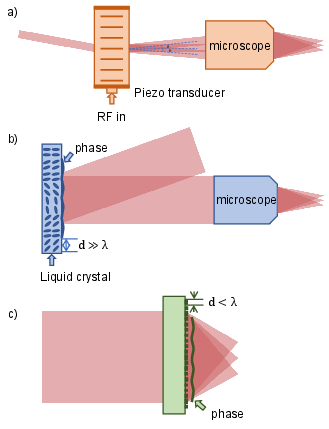
- Acousto-optic deflector (AOD): A device that uses sound waves in a crystal to diffract and steer laser beams. "A pair of AODs uses radio-frequency signals to produce acoustic waves that diffract the incident light into a two-dimensional array."
- Airy disk: The diffraction-limited focal spot pattern of a circular aperture, characterized by a central bright region and rings. "Simulations show that the metasurface can generate optical tweezers with an Airy disk radius of ."
- Block-wise FFT: A method to perform Fast Fourier Transforms on data larger than memory by processing it in smaller blocks. "To address this issue, we adopted a block-wise FFT approach."
- Chromium hard mask: A durable metal layer used as an etch mask during nanofabrication. "Subsequently, a chromium hard mask is formed through electron beam evaporation and lift-off."
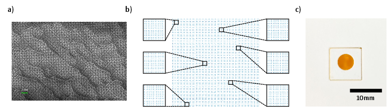
- CMOS-compatible process: A fabrication flow compatible with standard semiconductor manufacturing used for integrated circuits. "The metasurfaces are fabricated on fused-silica substrates using a CMOS-compatible process."
- Diffraction efficiency: The fraction of incident light power that is diffracted into a desired order by an optical element. "the finite pixel count and limited diffraction efficiency of SLMs."
- Diffraction-limited: A performance regime where spot size and resolution are limited only by fundamental optical diffraction, not aberrations. "the spots display near-diffraction-limited characteristics"
- Electron beam evaporation: A vacuum deposition technique where an electron beam melts a source material to form thin films. "Subsequently, a chromium hard mask is formed through electron beam evaporation and lift-off."
- Electron beam lithography: A high-resolution patterning method that writes nanostructures using a focused electron beam. "A poly(methyl methacrylate) resist is then spin-coated and patterned by electron beam lithography."
- Field of view (FOV): The spatial extent an imaging system can capture at once. "The intensity distribution at the focal plane was then imaged by a high-numerical-aperture (NA = 0.65) microscope objective with a $0.45$~mm field of view and relayed to a high-resolution CCD camera for analysis."
- Finite-Difference Time-Domain (FDTD): A numerical method for solving Maxwell’s equations by discretizing space and time. "obtained through Finite-Difference Time-Domain (FDTD) simulations"
- First diffraction order: The primary nonzero angular output of a diffractive element where light is directed after diffraction. "Measurement of the light utilization efficiency shows that 67.5\% of the incident light on the metasurface is diffracted into the first diffraction order"
- Fused silica: A high-purity glass with low optical loss, used as a substrate for high-performance optics. "a $5~$mm-diameter metasurface on a fused-silica substrate."
- High-numerical-aperture (NA): Refers to lenses with large NA that can focus light to small spots and collect light over wide angles. "The intensity distribution at the focal plane was then imaged by a high-numerical-aperture (NA = 0.65) microscope objective with a $0.45$~mm field of view and relayed to a high-resolution CCD camera for analysis."
- Inductively coupled plasma (ICP) etching: A plasma-based process for anisotropic, high-aspect-ratio etching of materials. "The pattern is transferred into the silicon nitride layer by inductively coupled plasma etching, followed by dry etching to remove the chromium mask."
- Lift-off: A fabrication technique where deposited material on resist is removed, leaving patterned films only on exposed areas. "Subsequently, a chromium hard mask is formed through electron beam evaporation and lift-off."
- Light utilization efficiency: The proportion of incident optical power that contributes to the intended output pattern. "These two effects yield a final light utilization efficiency of 58.8\%."
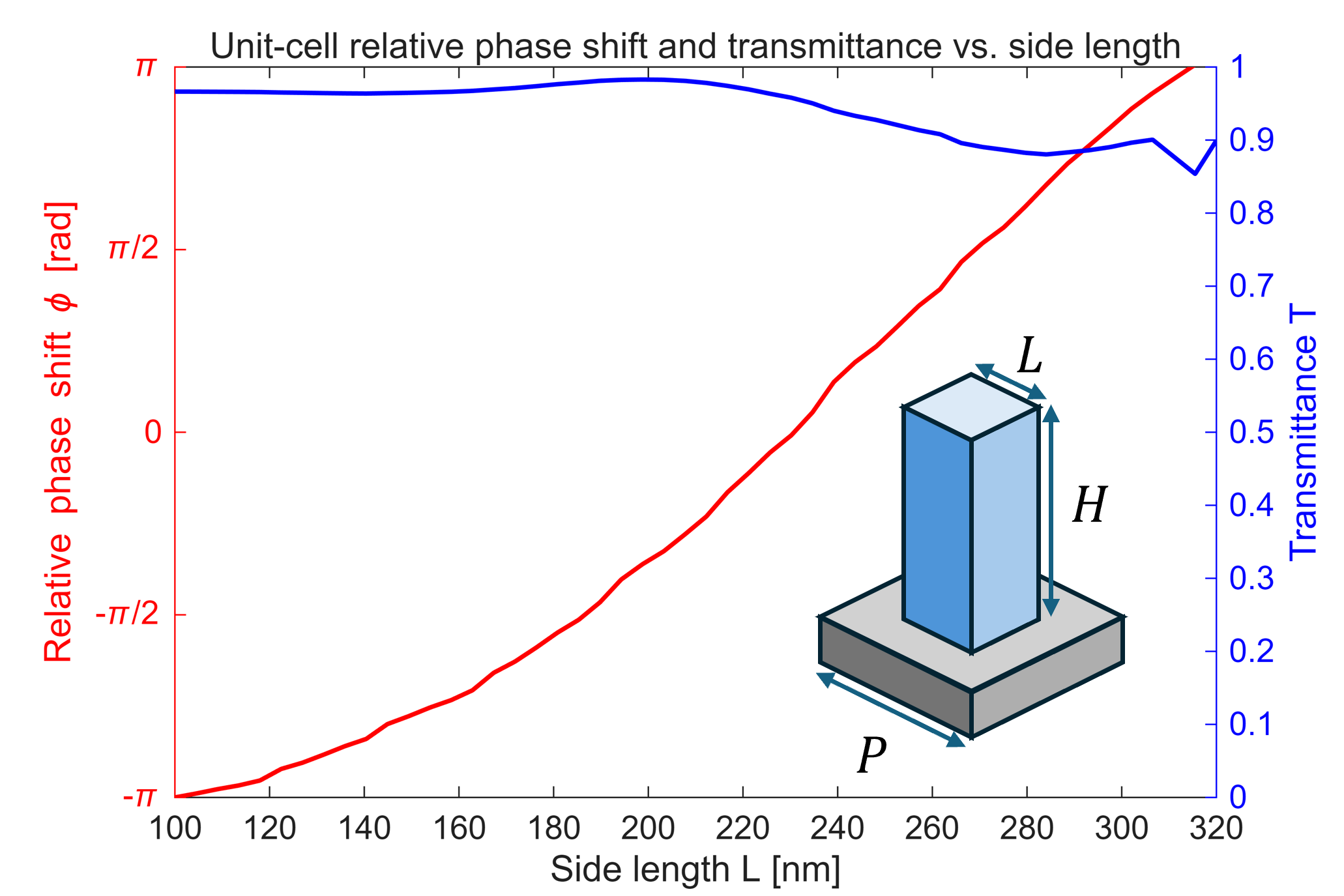
- Meta-atom: A subwavelength building block of a metasurface that imparts a designed phase, amplitude, or polarization change. "The metasurface is constructed using meta-atoms, square nanopillars made of silicon-doped silicon nitride."
- Metasurface: A planar array of engineered subwavelength structures that controls the phase, amplitude, and polarization of light. "A metasurface is a planar optical device composed of subwavelength nanostructures, known as meta-atoms, that can be individually engineered to modulate the phase, amplitude, and polarization of an incident light field"
- Near-neighbor coupling: Unintended optical interactions between adjacent nanostructures that affect device performance. "likely due to fabrication imperfections in the meta-atoms, near-neighbor coupling effects and interference with the undiffracted light."
- Numerical aperture (NA): A dimensionless measure of a lens’s ability to gather light and resolve fine detail. "Compared to the designed numerical aperture (NA) of 0.58, this measured radius corresponds to an effective NA of 0.51 at the operating wavelength of 852 nm."
- Optical tweezer: A tightly focused laser beam that uses gradient forces to trap microscopic particles or atoms. "Here, we demonstrate the experimental generation of an optical tweezer array containing spots using a metasurface"
- Phase hologram: A spatial phase pattern that shapes light into desired intensity distributions via interference and diffraction. "An SLM generates arbitrary patterns by encoding a phase hologram on a pixelated liquid-crystal array."
- Plasma-enhanced chemical vapor deposition (PECVD): A thin-film deposition method that uses plasma to enhance chemical reactions at lower temperatures. "depositing a silicon nitride layer via plasma-enhanced chemical vapor deposition."
- Point spread function (PSF): The response of an imaging system to a point source, describing its resolution and aberrations. "To characterize the quality of each tweezer, we perform an analysis of the point spread function"
- Polarization-independent operation: Device behavior that is insensitive to the polarization state of incident light. "The combination of the square pillar shape and square lattice geometry provides cross-sectional symmetry, enabling polarization-independent operation."
- Refractive index: A material parameter describing how much light slows and bends when entering the medium. "The silicon doping ratio in silicon nitride is optimized to achieve a refractive index of $2.3$."
- Scalar angular spectrum method: A computational technique for propagating optical fields by decomposing them into plane-wave components (scalar approximation). "Both forward and backward propagations are performed using the scalar angular spectrum method."
- Silicon nitride: A robust dielectric material used for nanophotonic structures due to its refractive properties and fabrication compatibility. "This well-established process robustly yields high-aspect-ratio silicon nitride nanopillars with aspect ratios exceeding $11:1$"
- Spatial light modulator (SLM): A pixelated device that modulates the phase (or amplitude) of light to form programmable patterns. "Currently, the optical tweezers in atom array platforms are commonly generated using acousto-optic deflectors (AODs) or spatial light modulators (SLMs)"
- Strehl ratio: A metric of optical quality comparing the peak focal intensity to that of a perfect (diffraction-limited) system. "over 99.7\% of the spots exhibiting Strehl ratios above 0.8."
- Subwavelength: Refers to structures smaller than the wavelength of light, enabling fine control of optical fields. "An optical metasurface directly shapes the wavefront of light via a dense array of subwavelength nanostructures"
- Transmittance: The fraction of incident light power transmitted through an optical element. "Plot of the relative phase shift (left axis) and transmittance (right axis) of a single meta-atom as a function of meta-atom size , obtained via FDTD simulations."
- Undiffracted light: The portion of light that passes through an optical element without being diffracted into designed orders. "likely due to fabrication imperfections in the meta-atoms, near-neighbor coupling effects and interference with the undiffracted light."
- Wavefront: The surface of constant phase of a propagating light field, whose shape determines focusing and interference. "leverages a large number of subwavelength phase-control pixels to engineer the wavefront of the incident light"
- Weighted Gerchberg-Saxton (WGS) algorithm: An iterative phase-retrieval method (with weighting) used to design holographic phase profiles for target intensity patterns. "We employ the Weighted Gerchberg-Saxton (WGS) algorithm to iteratively compute the phase profile at the metasurface required for generating the target optical tweezer array at the focal plane."
Collections
Sign up for free to add this paper to one or more collections.