- The paper introduces SINA, a fully automated schematic-to-netlist conversion method that achieves a 96.67% accuracy rate by integrating deep learning, VLMs, and OCR for both IC and PCB schematics.
- The paper demonstrates robust component detection and crossing-wire disambiguation, achieving up to 98% average precision and eliminating false positives in netlist reconstruction.
- The paper’s comprehensive pipeline, combining object detection, hybrid reference extraction, and graph isomorphism validation, paves the way for scalable analog and mixed-signal design automation.
SINA: Automated Schematic Image to Netlist Conversion with AI
Introduction
The automation of schematic-to-netlist conversion is a critical challenge in Electronic Design Automation (EDA), especially for analog and mixed-signal workflows where the bulk of existing design knowledge resides in circuit images scattered across publications, textbooks, and web resources. SINA ("Schematic Image-to-Netlist Automation") presents a comprehensive, open-source solution that integrates state-of-the-art deep learning, vision-LLMs (VLMs), and advanced image processing for fully automated schematic image interpretation spanning both Integrated Circuit (IC) and Printed Circuit Board (PCB) domains (2607.01609).
SINA’s contributions include robust IC/PCB domain generalization, superior component detection using YOLOv11 and VLM cross-verification, dedicated crossing-wire disambiguation, and accurate assignment of reference designators through hybrid OCR+VLM approaches. The pipeline demonstrates substantial performance gains—yielding a 96.67% netlist generation accuracy, a significant improvement over existing methods.
SINA Pipeline Overview
The SINA framework consists of four main sequential stages: component detection, connectivity inference, reference designator extraction/assignment, and netlist generation. This modular design ensures that errors in one stage are flagged or mitigated through subsequent cross-checks or VLM interventions.
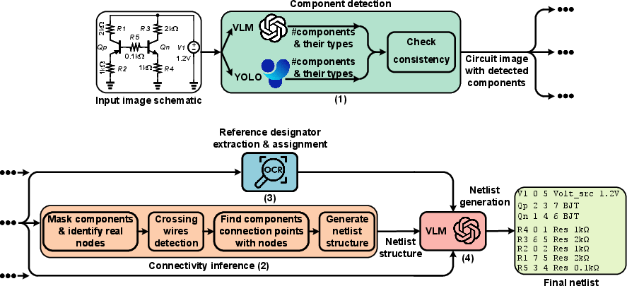
Figure 1: SINA workflow outlining the four primary stages: detection, connectivity, reference extraction/assignment, and netlist synthesis.
Component Detection with Hybrid Verification
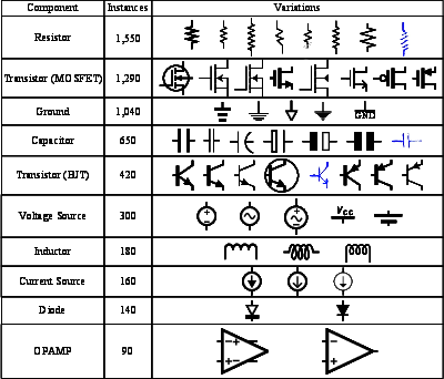
For component detection, SINA employs a YOLOv11-based model fine-tuned across diverse IC and PCB schematics, including hand-drawn variants. The model generates bounding boxes and class labels that are then cross-validated using a state-of-the-art VLM (GPT-4o) operating deterministically. Detected discrepancies between the two modalities trigger user review, maximizing reliability, especially for unseen or out-of-distribution symbols.
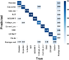
Strong numerical results support this two-pronged approach: the IC-level component detector achieves 93% precision, 99% recall, and a 96% F1 score, with a weighted mean average precision of 98%. VLM verification enhances robustness against both visually ambiguous and noisy images.

Figure 2: SINA pipeline applied to an IC-level schematic, from component detection and node clustering to the final netlist.
Connectivity Inference and Crossing-Wire Disambiguation
SINA's connectivity inference avoids fragile heuristics by applying Connected-Component Labeling (CCL) to images with components masked out, extracting candidate nets (nodes). Post-processing merges electrically equivalent nodes and excludes spurious artifacts by enforcing minimum connectivity constraints.
The framework addresses a major structural failure mode prevalent in competitor systems: ambiguity between crossing and connected wires. SINA's dedicated morphological and contour-based analysis identifies all perpendicular crossings. For each crossing, dual modified images are generated, each preserving only one of the two candidate connections. This results in accurate netlist reconstruction where false shorts from visual crossings are systematically excluded.
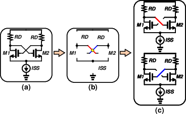
Figure 3: Stepwise illustration of SINA's crossing-wire detection and disambiguation process.
PCB-Level Schematic Processing
Detection and pin identification in PCB-level diagrams are more complex due to the prevalence of rectangular discrete components with variable pin layouts. SINA preprocesses images, inpainting out text, before employing both object detection and pose estimation YOLO variants. Experimental comparisons reveal that pose estimation models (YOLOv8m-pose) outperform detection-only models, yielding mAP50-95 of 94%, 94% precision, and 98% recall for components.
Pin identification leverages the Skeleton-OCR method, enabling robust endpoint extraction in noisy and occluded scenarios. This approach achieves a 95.3% F1 score compared to 43.6% via heuristic edge scanning.
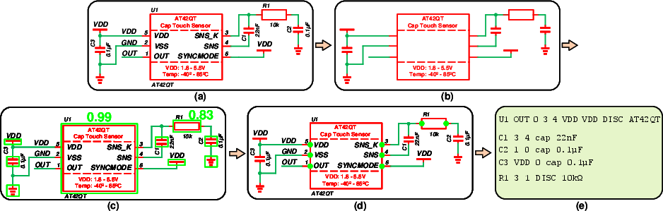
Figure 4: SINA workflow on a PCB-level schematic, highlighting text removal, component detection, pin extraction, and netlist generation.
Reference Designator Extraction and Assignment
SINA integrates EasyOCR for initial text extraction, following image preprocessing (contrast enhancement, denoising, adaptive thresholding). This reliably retrieves reference designators and parameter values, which are then spatially assigned to components. Final disambiguation and assignment occur through GPT-4o, which synthesizes visual and textual context for error correction, outperforming VLM-only extraction pipelines faced with typographically or spatially ambiguous schematics.
Netlist Generation and Topology Validation
The final machine-readable netlist is synthesized via GPT-4o using component-node mappings and OCR-extracted labels/values. Structural correctness is assessed through a rigorous graph isomorphism procedure, mapping both generated and ground truth netlists to bipartite graphs and evaluating their equivalence up to relabeling and reordering.
Experiments show SINA outperforms Masala-CHAI [bhandari2024masala] by a factor of 2.72x in holistic netlist generation accuracy (96.67% vs. 35.5%), with dramatic improvements in both component detection and circuit structure fidelity.
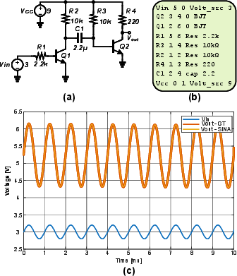
Figure 5: Example where SINA's netlist is an exact match to ground truth, validated via simulation.
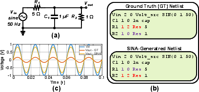
Figure 6: A case where the SINA netlist is topologically equivalent but not an exact match, illustrating subtle differences in generated connectivity.
Evaluation: Numerical Results and Functional Validation
The evaluation methodology leverages diverse benchmarks: more than 700 annotated schematics for training, with thorough breakdowns by component type, instance count, and complexity (Figures 5 and 6). Performance is decomposed into:
Implications and Future Directions
SINA’s architecture demonstrates that robust, fully automated schematic-to-netlist conversion is feasible using hybrid deep learning and VLM paradigms. This unlocks large-scale extraction of verified analog and PCB circuit knowledge from visual corpora, supporting downstream simulation, verification, and AI-based synthesis workflows. The crossing-wire disambiguation strategy resolves a long-standing source of structural errors in generated netlists, promoting direct adoption of visual design assets for machine learning and design reuse.
The framework’s open-source implementation, combined with rigorous structural and functional validation mechanisms, establishes a reproducible benchmark for future research. Prospective directions include tighter VLM-vision model integration, expansion toward non-traditional schematic domains (multi-sheet, hierarchical), and domain-adaptive data augmentation to further improve generalization.
Conclusion
SINA provides a comprehensive, scalable pipeline for transforming arbitrary circuit schematics—across both IC and PCB domains—into accurate, simulation-ready netlists. By fusing deep object detection, hybrid reference designator extraction, and innovative crossing-wire disambiguation, SINA sets a new standard for robust schematic interpretation. Its demonstrated accuracy and functional reliability pave the way for the large-scale curation of circuit knowledge repositories and enable the next generation of AI-driven analog and mixed-signal design automation.