Imaging of induced surface charge distribution effects in glass vapor cells used for Rydberg atom-based sensors
Abstract: We demonstrate the imaging of localized surface electric (E) field effects on the atomic spectrum in a vapor cell used in Rydberg atom-based sensors. These surface E-fields can result from an induced electric charge distribution on the surface. Induced surface charge distributions can dramatically perturb the atomic spectrum, hence degrading the ability to perform electrometry. These effects become pronounced near the walls of the vapor cell, posing challenges for vapor cell miniaturization. Using a fluorescence imaging technique, we investigate the effects of surface charge on the atomic spectrum generated with electromagnetically induced transparency (EIT). Our results reveal that visible light (480 nm and 511 nm), i.e., the coupling laser used in two-photon Rydberg EIT schemes, generates localized patches of charge or dipoles where this light interacts with the glass walls of the vapor cell, while a three-photon Rydberg EIT scheme using only near-infrared wavelength lasers shows no measurable field induction. Additionally, imaging in a vacuum chamber where a glass plate is placed between large electrodes confirms that the induced charge is positive. We further validate these findings by studying the photoelectric effect with broadband light during EIT and impedance measurements. These results demonstrate the power of the fluorescence imaging technique to study localized E-field distributions in vapor cells and to target the photoelectric effect of the alkali-exposed glass of vapor cells as a major disruptor in Rydberg atom-based sensors.
Paper Prompts
Sign up for free to create and run prompts on this paper using GPT-5.
Top Community Prompts
Explain it Like I'm 14
Overview
This paper looks at a problem that happens inside special glass cells used for super-sensitive electric field sensors based on “Rydberg atoms.” Rydberg atoms are atoms with one electron very far from the nucleus, which makes them act like tiny, ultra-sensitive antennas for electric fields. The researchers discovered that certain colors of light can make little “patches” of electric charge appear on the inner glass walls of these cells. These charge patches create electric fields that disturb the atoms and mess up the sensor’s readings. The paper shows a way to “see” where those charge patches are, explains what causes them, and suggests how to avoid the problem.
What questions were they asking?
- Do the lasers used in these sensors create unwanted electric charges on the glass walls?
- If so, where exactly do these charges appear, how strong are they, and what color (wavelength) of light causes them?
- Are these charges positive or negative?
- Can we run the sensor in a way that avoids creating these charges?
How did they study it? (Methods explained simply)
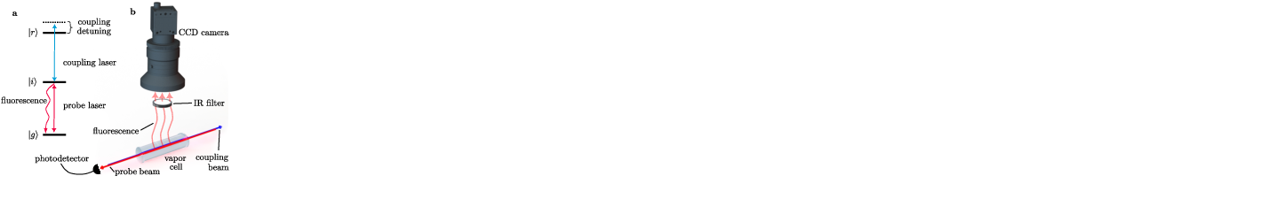
The team used a clever “glow camera” method to watch how the atoms behave along the path of a laser inside the glass cell:
- Electromagnetically Induced Transparency (EIT): Think of EIT like a lock-and-key trick with atoms. When two or three lasers are tuned just right, the atoms stop absorbing light and become more transparent. If an electric field is present, it nudges the atoms’ energy levels, and the “just right” condition shifts. By scanning the laser frequency, you can see where the atoms change their glow and how much they’ve been nudged.
- Fluorescence imaging: As the laser frequency is scanned, the atoms’ glow (fluorescence) changes. A camera takes a picture of that glow along the laser’s path. This turns the glass cell into a one-dimensional “map,” showing where electric fields are stronger or weaker. It’s like using a night-vision camera to see hot and cold spots, except here it’s electric-field “hot spots.”
They ran several experiments:
- Two-photon EIT (uses visible blue/green light around 480–511 nm) and three-photon EIT (uses only near-infrared light, no visible light).
- A “re-entry” test: they bounced the visible laser back onto the side of the cell at different locations to see if that specific spot would charge up.
- A vacuum-chamber test with metal plates and a glass sample to figure out the charge’s sign (positive or negative).
- A broadband light test: they shined many different wavelengths (colors) to find out which ones cause charging.
- Electrical measurements (impedance) to check whether the glass itself or the alkali metal on the glass is responsible.
Terms in everyday language:
- Rydberg atom: an atom with a “very stretched-out” electron, making it super sensitive to electric fields.
- Electric field: an invisible force field created by electric charges.
- Surface charge: extra positive or negative charges that collect on a surface.
- Photoelectric effect: light knocking electrons off a material, which can leave behind positive charges.
What did they find and why it matters?
Here are the main findings:
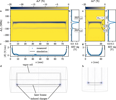
- Visible light creates charge patches on the glass where the light hits. When they used blue/green light (about 480–511 nm), the glass cell developed localized positive charges at the laser entry/exit points. These charges created electric fields that shifted the atoms’ signals, especially near the walls.
- The effect is local and strong near the wall. The electric field is strongest right where the light hits and then fades as you move away. In small cells (short laser paths), these wall effects can dominate the measurement, making it hard to get clean, accurate readings.
- More light power makes more charging (up to a point). Increasing the visible laser power increased the amount of charge and the strength of the unwanted electric field, showing a saturation behavior at higher powers.
- The induced charge is positive. In the vacuum-chamber test, applying an external voltage showed that the added field either helped or fought against the induced field in a way that proves the surface charge is positive. That fits with the photoelectric effect: light kicks off electrons and leaves behind positive ions.
- The wavelength threshold matches the photoelectric effect of alkali metals. The charging happened for light with wavelengths shorter than about 600–650 nm (higher-energy light). That energy range matches published “work function” values for cesium (1.9–2.1 eV), meaning it’s the alkali metal (like cesium or rubidium) coating the glass that’s being photo-ionized, not the bare glass itself.
- Three-photon EIT (all near-infrared) avoids the problem. When they used only near-infrared lasers (no visible light), they saw little to no charging. But as soon as they added a small amount of blue light, the charging returned.
Why this matters:
- These charge patches distort the atom signals the sensor relies on. That hurts sensitivity and accuracy, especially when trying to build small, chip-scale devices. Knowing the cause and how to avoid it is key for making practical, reliable Rydberg-based sensors.
Why this matters for the future (Implications)
- Design sensors to avoid visible light on the glass: Using three-photon (near-infrared) laser schemes can greatly reduce charging, leading to cleaner, more stable measurements.
- Better small sensors: Because the problem is strongest near walls, it’s especially important for miniaturized devices. This work points the way to making tiny, high-performance Rydberg sensors for communications, imaging, and environmental sensing.
- A new diagnostic tool: The “glow camera” (fluorescence imaging) method gives a powerful way to see where unwanted electric fields are inside the cell. This can guide better cell designs, coatings, and manufacturing steps to reduce charging.
- Future improvements: With better signal processing (like lock-in detection) and control of laser polarization, researchers can measure even weaker fields and figure out whether surface effects are from true charges or from dipoles (charge pairs).
In short, the paper shows that blue/green light can create unwanted positive charges on the inside of glass vapor cells, disturbing the delicate measurements that Rydberg-atom sensors make. By switching to near-infrared light and using imaging to map where fields appear, researchers can avoid or fix these issues, paving the way for better, smaller, and more reliable electric-field sensors.
Collections
Sign up for free to add this paper to one or more collections.