- The paper presents a scalable flip-chip bonding method for integrating 450-nm InGaN lasers with SiN waveguides, achieving high on-chip power up to 60.7 mW.
- The study employs sub-micron alignment precision and compares inverse taper versus partially-etched taper designs, showing coupling losses as low as 1.1 dB.
- The work validates a foundry-compatible visible-light PIC design, establishing a platform for AR/VR, quantum photonics, and biosensing applications.
Introduction and Motivation
The integration of efficient visible-wavelength light sources into silicon photonic platforms is a critical enabler for a range of emerging applications, including quantum information processing, biosensing, and augmented/virtual reality. While silicon photonics has matured for near-infrared applications, extending these platforms into the visible spectrum introduces new challenges, particularly in the integration of direct-bandgap semiconductor lasers with silicon nitride (SiN) waveguides. The indirect bandgap of silicon and the wide bandgap of SiN preclude efficient on-chip light generation, necessitating hybrid integration of III-V semiconductor lasers. This work demonstrates passive-alignment flip-chip bonding of 450-nm InGaN laser diodes (LDs) onto a foundry-fabricated visible-light Si photonics platform, achieving high coupling efficiency, scalable assembly, and robust device performance.
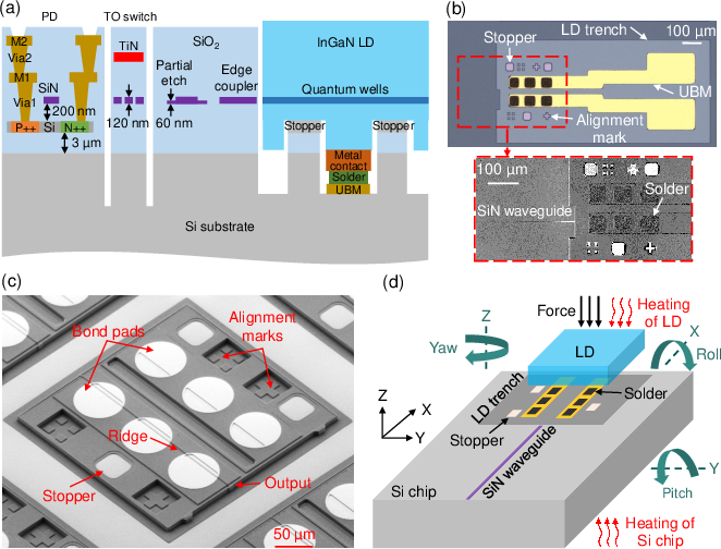
Figure 1: Hybrid integration of InGaN laser diodes (LDs) in a visible-light Si photonics platform, showing platform cross-section, bonding socket micrographs, LD top surface, and flip-chip bonding concept.
The photonic platform is fabricated on 200-mm SOI wafers and incorporates SiN waveguides, thermo-optic (TO) switches, and waveguide-coupled Si photodetectors. The process flow includes Si photodetector formation, SiN waveguide definition via DUV lithography and RIE, metallization for routing and heaters, and the creation of bonding sockets with lithographically defined alignment marks and mechanical stoppers. Under-bump metallization (UBM) and AuSn solder bumps are patterned within the sockets for electrical and thermal interfacing with the LDs.
The InGaN LDs, fabricated by ams OSRAM, are co-designed for hybrid integration, featuring etched alignment marks and mechanical stoppers to match the Si photonic chip. Both P and N contacts are on the top side, facilitating electrical connection via flip-chip bonding. The LD emission is edge-coupled into SiN waveguides using either inverse taper or taper coupler designs, optimized for mode matching and alignment tolerance.
Flip-Chip Bonding Methodology
A semi-automated die bonder with sub-micron placement accuracy is employed for passive-alignment flip-chip bonding. The process utilizes a heatable vacuum pickup tool and a vision alignment system to overlay alignment marks on the LD and Si chip, ensuring precise in-plane and vertical positioning. Localized heating enables sequential integration of multiple LDs on a single chip without global thermal exposure.
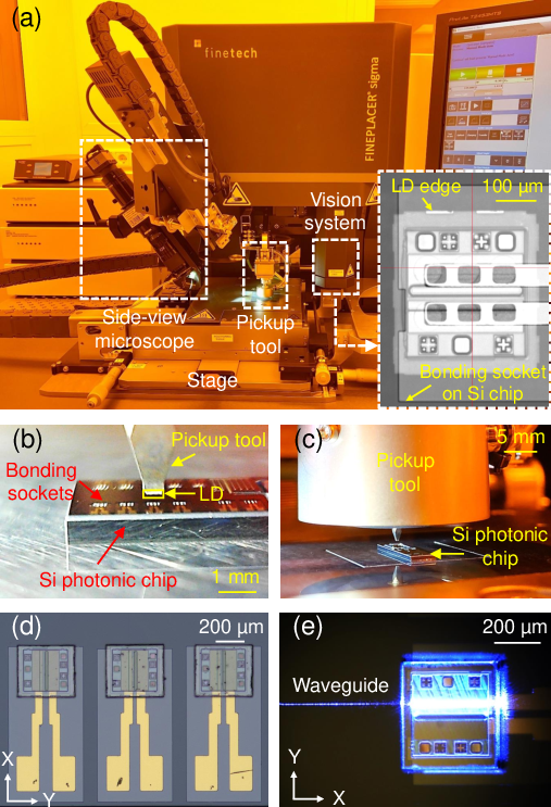
Figure 2: Flip-chip bonding technique, including die bonder setup, LD approach, pickup tool, multiple bonded LDs, and light coupling into SiN waveguide.
The bonding process involves pre-heating both chips, aligning via vision system, touchdown with controlled force, thermocompression bonding at 400°C (tool) and 270°C (stage), and controlled cooling. The process achieves a cycle time of ~15 minutes per LD.
Optical Coupling and Alignment Sensitivity
Two coupler geometries are evaluated: a full-thickness SiN inverse taper and a partially-etched SiN taper. Simulations using FDE and 3D FDTD solvers yield coupling losses of 2.9 dB (inverse taper) and 0.6 dB (taper) under ideal alignment. The 3-dB misalignment tolerances are sub-micron, with the taper design offering higher efficiency but increased sensitivity to X and Z misalignments.
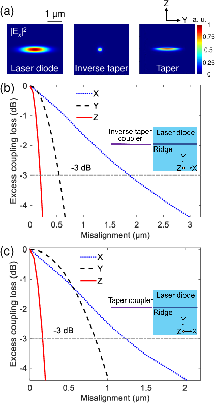
Figure 3: Simulated mode profiles and misalignment tolerance for inverse taper and taper couplers at 450 nm.
Bonding Process Characterization
A statistical study of 40 bonded LDs (20 per coupler type) quantifies post-bonding in-plane misalignment and on-chip optical power. Confocal laser scanning microscopy through the transparent LD substrate enables direct measurement of alignment mark offsets. The standard deviations are 635 nm (X) and 665 nm (Y), with 85% of samples within ±1 μm. Rotational misalignment is minimal (<0.2°), as confirmed by white light interferometry.
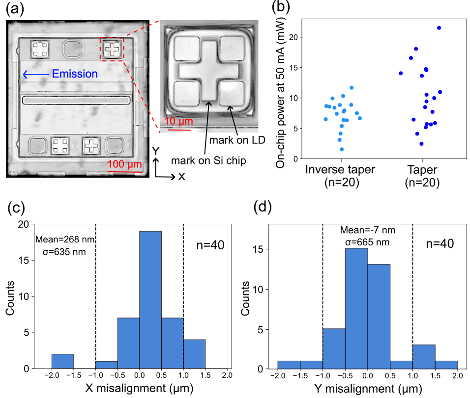
Figure 4: Post-bonding alignment characterization, on-chip power distribution, and misalignment histograms for 40 bonded LDs.
Measured coupling losses are 4.1 dB (inverse taper) and 1.1 dB (taper), with maximum on-chip powers of 7.5 mW and 10.5 mW, respectively. The observed variability is attributed to the tight alignment tolerances at visible wavelengths and the die bonder's placement accuracy.
The highest measured on-chip optical power is 60.7 mW, with a wall-plug efficiency (WPE) of 7.8%, representing a new benchmark for hybrid-integrated visible-spectrum lasers. L-I-V characterization shows stable operation up to 185 mA drive current, with device failure attributed to high current density. Thermal rollover is observed in some devices at >130 mA.
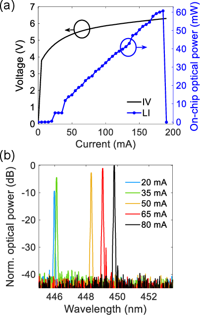
Figure 5: L-I-V curves and optical spectra for the highest-power flip-chip bonded LD.
Epoxy underfill and encapsulation (PDMS and thermally conductive epoxy) yield a moderate average power increase of 12.6%, attributed to reduced Fresnel reflection and improved heat dissipation. The flip-chip process induces only minor changes in LD series resistance and emission power.
Temperature-dependent measurements show a threshold current increase from 16 mA to 22 mA and a 15.5% power drop at 80°C, with a characteristic temperature of 187 K. The emission wavelength red-shifts with temperature, and the spectral linewidth remains <0.1 nm.
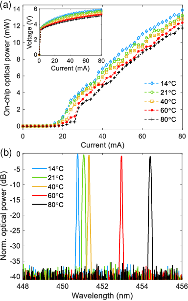
Figure 6: Temperature-dependent L-I-V curves and emission spectra for a representative flip-chip bonded LD.
Photonic Integrated Circuit Demonstration
A proof-of-concept PIC integrates a flip-chip bonded LD, a waveguide-coupled photodetector, and a TO switch. The circuit supports optical switching between two outputs with >23 dB extinction ratio and variable optical attenuation over 13 dB without wavelength shift. The integrated photodetector enables on-chip power monitoring under both DC and 1 MHz AC modulation, with the photocurrent tracking the LD current and off-chip optical power.
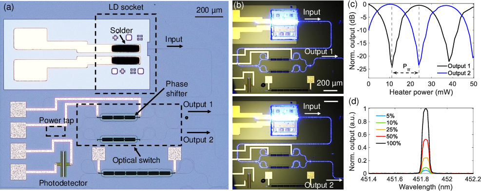
Figure 7: PIC with bonded LD, photodetector, and TO switch, demonstrating switching, attenuation, and spectral stability.
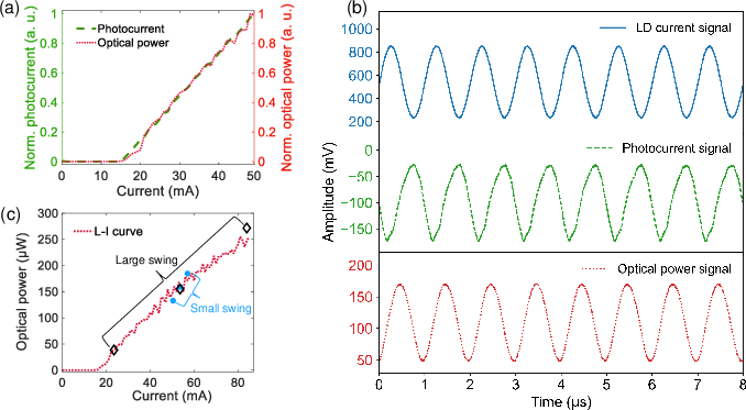
Figure 8: On-chip power monitoring using the integrated photodetector, showing DC and AC response and dynamic power tracking.
Comparative Analysis and Implications
This work achieves a minimum coupling loss of 1.1 dB and a maximum on-chip power of 60.7 mW, exceeding previous visible-spectrum hybrid integration demonstrations by a factor of six in power. The primary limitation is the variability in alignment and coupling efficiency, which can be mitigated by higher-precision die bonders and coupler designs with relaxed misalignment tolerances (e.g., multi-tip or adiabatic couplers). The platform supports integration of multiple LDs, enabling future wavelength-multiplexed or arrayed sources.
The demonstrated integration of LDs, photodetectors, and TO devices establishes a foundation for complex visible-light PICs. The approach is compatible with high-throughput manufacturing and is extensible to additional functionalities, such as MEMS beam scanners and high-speed photodetectors, supporting applications in AR/VR, quantum photonics, and biophotonics.
Conclusion
This work establishes a scalable, high-performance methodology for hybrid integration of visible-wavelength InGaN laser diodes onto foundry-fabricated Si photonic platforms via passive-alignment flip-chip bonding. The demonstrated sub-micron alignment, high on-chip power, and robust device operation validate the approach for advanced visible-light PICs. Future developments will focus on improving alignment precision, expanding wavelength coverage, and integrating additional active and passive components to enable fully integrated, multifunctional photonic systems for next-generation applications.